
Patterns of polar vortices detected in lead-free superlattices on silicon
HZB team thus expands the possibilities for novel ferroelectric components
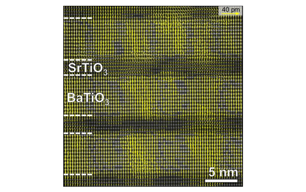
A team at HZB has, for the first time, reported polar vortices in (BaTiO3/SrTiO3)10 superlattices on silicon. These results expand the range of materials and substrates on which polar topological textures can occur and open up new options for incorporating complex ferroelectric states into silicon-based technologies.
Polar textures such as vortices have been so far observed almost exclusively in lead-containing superlattices comprising ultra-thin ferroelectric and dielectric titanate layers on oxide substrates. The delicate balance between electrical forces, mechanical stresses (imposed by the substrate), and the energy required to change the direction of polarization leads to distinctive electrical dipole patterns in the ferroelectric layers. In principle, structures with complex polar states could be used to develop novel components with specific functions, as the structures are small, stable and can be influenced by external electric fields. However, to achieve this, it would be important to replace the toxic lead and deposit the layers on silicon substrates, the ubiquitous platform of the semiconductor industry.
Superstructure on silicon
A team led by HZB physicist Prof. Dr. Catherine Dubourdieu has now succeeded in doing so: in their new study, published in Nature Communications, the team presents epitaxially grown alternating layers of barium and strontium titanates on silicon that exhibits regular stripes of polar vortices. The layer system was created with molecular beam epitaxy in the HZB Quantum Materials lab. Using the scanning transmission electron microscope from the group of Prof. Christoph Koch at Humboldt University and further analysis at the PETRA III X-ray source in Hamburg, they were able to demonstrate the superstructure consisting of regular ferroelectric vortex tubes.
Robust stripe pattern
The vortices in each BaTiO₃ layer align along a specific crystal direction of BaTiO3 and form a robust striped pattern. The silicon substrate provides the necessary mechanical strain, which enables the polar vortices to form. When the samples are heated, a structural phase transition occurs and the polar texture disappears. Upon cooling to room temperature, the polar texture reforms.
The function of strain explained
Phase-field modelling performed by the group of Prof. Long-Qing Chen at the Pennsylvania State University, USA, replicates the coupling of BaTiO₃ and SrTiO₃ layers via electrostatic forces and mechanical strain. This modelling also explains how the vortex tubes in the BaTiO3 layers align, providing insight into the development of the polar texture pattern as a function of strain.
“This is the first realisation of periodically ordered vortices in BaTiO3 superlattices on silicon. Actually, silicon is the key, as it provides the necessary strain to induce this vortex pattern,” says doctoral student Valentin Hevelke, first author of the study.
Expanding the range of materials
“Our results expand the range of materials and substrates on which polar topological textures can occur and open up new options for incorporating complex ferroelectric states into silicon-based technologies,” says Catherine Dubourdieu.
Note: This study is funded by the ERC Advanced Grant LUCIOLE.
Publication:
Nature communications (2026): Periodic polar vortices in BaTiO3/SrTiO3 superlattices monolithically grown on silicon
Valentin Väinö Hevelke, Ines Häusler, Aiden Ross, Israel Ibukun Olaniyan, Sven Wiesner, Minh Anh Luong, Leifeng Zhang, Sylvie Schamm-Chardon, Kristiane Elsner, Benedikt Haas, Adnan Hammud, Florian Bertram, Christoph T. Koch, Long-Qing Chen, Dong-Jik Kim & Catherine Dubourdieu.
DOI: 10.1038/s41467-026-77270-0
Contact:
Helmholtz-Zentrum Berlin für Materialien und Energie
Institute Functional Oxides for Energy-Efficient IT
Prof. Dr. Catherine Dubourdieu
(030) 8062 - 42868 / (030) 8062 - 15802
catherine.dubourdieu(at)helmholtz-berlin.de
Press Officer
Dr. Antonia Rötger
(030) 8062-43733
antonia.roetger(at)helmholtz-berlin.de
HZB press release, 19.10.2026