• Skip to Management
  • Skip to Main menu
  • Skip to Page content
Adlershof Logo
  • WISTA
  • WISTA.Plan
  • WISTA.Service
WISTA direkt
Search
  • de
  • en
  • Adlershof Logo
  • About / Directory
    • Companies / Institutes
    • Science City in numbers
    • Direction / Maps
      • Bus / Train
      • By Car
      • Bicycle
      • Orientation / Maps
      • Trail of Thoughts
  • Newsroom
    • Overview
    • News
      • Social Media Stream
      • Success Stories
    • Events / Calendar
      • Adlershof Dissertation Award
      • Adlershof Research Forum
      • Long Night of Sciences Berlin
    • Adlershof Journal
    • Hot Topics
      • Adlershof Mission "Grand Challenges"
      • Circular Economy
      • Digital infra­structure / 5G campus network
    • Photos / Flyer / Downloads
      • Magazine archive
    • WISTA-Editorial Staff
  • Science / Technology
    • Overview
    • Technology Centres
      • Photonics / Optics
      • Biotech­nology / Envi­ron­ment
      • Micro­systems / Materi­als
      • IT / Media
      • Renewable Energy / Photovoltaics
    • Non-university Research
    • Universities / Colleges
      • Humboldt-Universität zu Berlin
      • Services for Students
    • Young Talents / STEM / School Labs
    • Start-Ups
      • Adlershof Start-Up Centre IGZ
      • Adlershof Founder’s Lab
    • Networks / Management
      • Campus Club Adlershof
  • TV / Media
    • TV and Movie Production
    • Media Services / Companies
    • News and Events
    • Filming Locations
    • Costume Hire
    • GDR Film Archive
    • Tickets / Booking
  • Properties
    • Overview
    • Real Estate Rent
      • Office Space / Workspace / Laboratories
    • Real Estate Offers
      • Commercial Properties
    • ST3AM Working Environments / Coworking
    • Residential
    • Construction
      • Building Projects
      • Architecture
      • Webcam
  • Service
    • Overview
    • Gastronomy / Sport / Culture / Shopping
    • Jobs / Market
    • Social and Healthcare Facilities
    • WISTA-Business Services
    • Event Services / Guided Tours / Hotels
    • Facility Management
    • Downloads / Photos / Videos
    • Jobs for Refugees
  • Hood
    • Overview
    • History
    • Nature Park
    • Culture
    • Technology Park
    • Digital Tours
  • WISTA
  • WISTA.Plan
  • WISTA.Service
WISTA direkt

Events / Calendar

  • Overview
  • News
  • Events / Calendar
  • Adlershof Journal
  • Hot Topics
  • Photos / Flyer / Downloads
  • WISTA-Editorial Staff
  • Adlershof
  • Newsroom
  • Events / Calendar
27. August 2019

Gallium oxide power transistors with record values

Ferdinand-Braun-Institut achieves breakthrough in the field of energy-efficient power electronics

Gallium oxide chip © FBH/schurian.com
Gallium oxide chip with transistor structures and structures for measurement purposes, manufactured at FBH using projection lithography © FBH/schurian.com

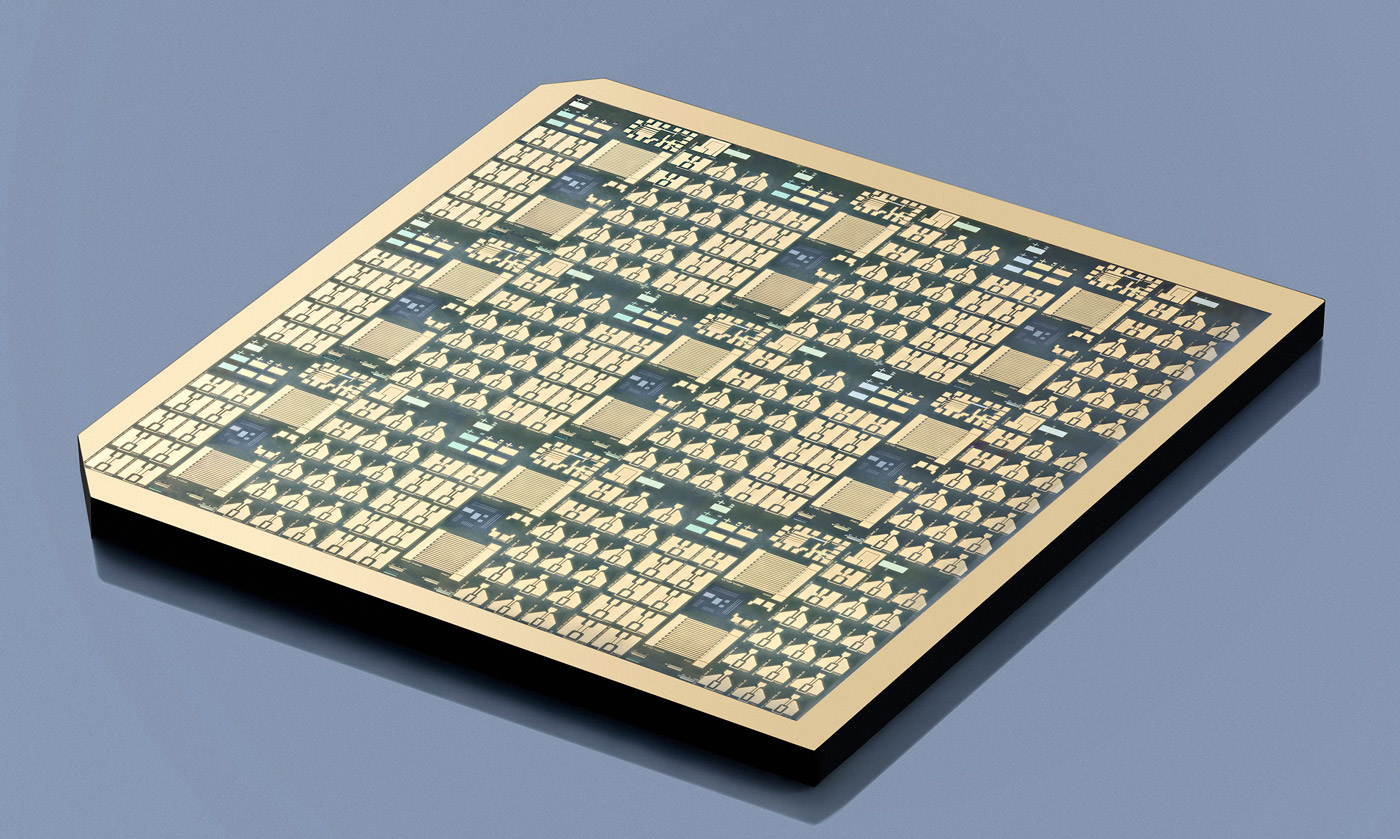
Powerful electronic components are indispensable for future communications, for the digital transformation of society and for artificial intelligence applications. On a footprint as small as possible, they should offer low energy consumption and achieve ever higher power densities, thus working more efficiently. This is where conventional devices reach their limits. Scientists all over the world are therefore investigating new materials and components that can meet these requirements. The Ferdinand-Braun-Institut (FBH) has now achieved a breakthrough with transistors based on gallium oxide (ß-Ga2O3).

The newly developed ß-Ga2O3-MOSFETs (metal-oxide-semiconductor field-effect transistor) provide a high breakdown voltage combined with high current conductivity. With a break-down voltage of 1.8 kilovolts and a record power figure of merit of 155 megawatts per square centimeter, they achieve unique performance figures close to the theoretical material limit of gallium oxide. At the same time, the breakdown field strengths achieved are significantly higher than those of established wide bandgap semiconductors such as silicon carbide or gallium nitride.

Optimized layer structure and gate topology

In order to achieve these improvements, the FBH team tackled the layer structure and gate topology. The basis was provided by substrates from the Leibniz Institute for Crystal Growth with an optimized epitaxial layer structure. As a result, the defect density could be reduced and electrical properties improved. This leads to lower on-state resistances. The gate is the central ‘switching point’ of field effect transistors, controlled by the gate-source voltage. Its topology has been further optimized, allowing to reduce high field strengths at the gate edge. This in turn leads to higher breakdown voltages. The detailed results were published online on August 26, 2019 in the IEEE Electron Device Letters September issue:

Lateral 1.8 kV ß-Ga2O3 MOSFET With 155 MW/cm2 Power Figure of Merit
Kornelius Tetzner; Eldad Bahat Treidel; Oliver Hilt; Andreas Popp; Saud Bin Anooz; Günter Wagner; Andreas Thies; Karina Ickert; Hassan Gargouri; Joachim Würfl
IEEE Electron Device Letters (Volume: 40, Issue: 9, Sept. 2019)
 

Contact

Petra Immerz, M.A.
Communications Manager
Ferdinand-Braun-Institut, Leibniz-Institut für Höchstfrequenztechnik
Gustav-Kirchhoff-Straße 4, 12489 Berlin, Germany
Phone +49 30 6392-2626
Email petra.immerz(at)fbh-berlin.de
Web www.fbh-berlin.de

Research Photonics / Optics Microsystems / Materials

Related News

  • Gallium oxide chip ©FBH/schurian.com

    Joint project “ForMikro-GoNext” launched

    Semiconductor material beta-gallium oxide offers the best prerequisites for next-generation power electronics
  • HiPoSwitch: GaN switching transistors on silicon substrate

    Fast, efficient switching – thanks to HiPoSwitch

    FBH’s novel GaN switches for power converters save primary energy consumption

Related Institutions

  • Leibniz-Institut für Kristallzüchtung im Forschungsverbund Berlin e.V. (IKZ)
  • LinkedInshare0
  • Facebookshare0
  • WhatsAppshare0
  • E-Mail

The development of the Science and Technology Park Berlin Adlershof was and is co-financed by the European Union namely by EFRE. This concerns infrastructure development like construction of technology centres. Furthermore EFRE is used for international projects.

  • © WISTA Management GmbH
  • Legal Notice
  • Privacy Policy
  • Social Media Guide
  • FAQ
  • Contact
  • Press
  • Newsletter
  • RSS
  • International
Member of:
Zukunftsort Adlershof Logo