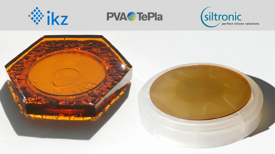
4-Inch Aluminum Nitride Crystals for Future Markets in Power Electronics and UV Photonics
Innovation project launched by IKZ, PVA TePla AG and Siltronic AG
Three leading players in semiconductor research and development – the Leibniz-Institut für Kristallzüchtung (IKZ), the PVA TePla AG, and the Siltronic AG – are combining their expertise in a pioneering project to scale up aluminum nitride (AlN) crystal growth. The project focuses on the fabrication of 4-inch AlN substrates to enable advanced applications in high-power electronics and ultraviolet photonics.
Aluminum nitride (AlN) is an ultra-wide bandgap (UWBG) semiconductor material characterized by outstanding intrinsic properties, including high critical electric field strength, superior thermal conductivity, and optical transparency in the ultraviolet spectrum. These attributes make AlN a highly promising substrate and device material for next-generation power electronic components and UV disinfection technologies, enabling compact, energy-efficient, and thermally robust device architectures.
The project's focus on scaling AlN crystal diameters from 2 to 4 inches addresses a fundamental requirement for transitioning this key material from research-scale to industrial manufacturing environments. The project is set to make a substantial contribution to advancing Europe's sovereignty in the field of semiconductor materials research. AlN-based power electronics enable major efficiency gains in electromobility, renewable energy, and industrial systems. In UV photonics, new opportunities arise in areas such as disinfection (preventing pandemics and water treatment), production technology (material processing), agriculture (yield enhancement), as well as sensors and medical applications.
The partners are leveraging their respective core competencies to jointly develop a market-ready technology for the industrial production of aluminum nitride crystals.
The Leibniz-Institut für Kristallzüchtung (IKZ) brings its long-standing expertise in growing AlN crystals to the project and has a proven 2-inch AlN crystal growth platform. Thanks to its leading position in producing high-quality AlN wafers, the institute is widely acknowledged as a European reference in this field of technology.
Siltronic AG, one of the world’s leading producers of silicon wafers (using both Czochralski and Float Zone methods), contributes its extensive experience in in the research and development of substrates for power electronics and in precision metrology – both of which are crucial for the industrial application of AlN wafers.
PVA TePla AG is an internationally leading provider of high-tech solutions in the fields of material and metrology technology with decades of experience in manufacturing crystal growing systems. With its expertise in the Physical Vapor Transport (PVT) method, particularly based on comprehensive experience from the SiC market, PVA TePla provides the technological equipment foundation for a reliable and reproducible growth process for bulk AlN crystals with industry-relevant diameters. This forms a central prerequisite for scaling and industrializing AlN technology.
Through their collaboration, IKZ, PVA TePla, and Siltronic are firmly demonstrating their commitment to Europe's technological sovereignty and the sustainable development of a semiconductor materials value chain. “The expansion from 2-inch to 4-inch is a crucial milestone in making AlN accessible for mass production”, the project partners explain. “Thanks to the synergies among the partners, we can overcome the technological barriers.”
Contact
Leibniz-Institut für Kristallzüchtung (IKZ)
Dr. Carsten Hartmann
Crystalline Materials for Electronics
Aluminum Nitride Prototyping
+49 30 246499-602
carsten.hartmann(at)ikz-berlin.de
Stefanie Grüber
Public Relations
+49 30 246499-126
stefanie.grueber(at)ikz-berlin.de
Joint press release by IKZ, PVA TePla and Siltronic, 26 June 2025
