Amplifier for terahertz lattice vibrations in a semiconductor crystal
MBI scientists see great potential for ultrasound imaging with a sub-nanometer spatial resolution
In analogy to the amplification of light in a laser, vibrations of a semiconductor crystal, so called phonons, were enhanced by interaction with an electron current. Excitation of a metal-semiconductor nanostructure by intense terahertz (THz) pulses results in a ten-fold amplification of longitudinal optical (LO) phonons at a frequency of 9 THz. Coupling such lattice motions to propagating sound waves holds potential for ultrasound imaging with a sub-nanometer spatial resolution.
The laser is based on a fundamental principle in physics, the (L)ight (A)mplification by (S)timulated (E)mission of (R)adiation. This concept theoretically predicted by Albert Einstein in 1916 and experimentally demonstrated for the first time in 1961 can be adopted for the phonon, a vibrational quantum in a crystal which consists of a regular arrangement or lattice of atoms in space. Phonons can be absorbed or emitted by electrons in the crystal. A net amplification of phonons requires that their number emitted per second via stimulated emission is larger than that absorbed per second. In other words, there must be more electrons emitting than absorbing a phonon.
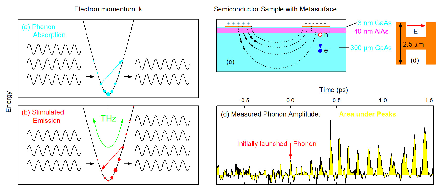
This condition is illustrated schematically in Fig. 1 where the electron energy is plotted as a function of the electron momentum k, following roughly a parabolic dependence. For a thermal equilibrium distribution of electrons at room temperature [sketched by filled blue circles of different size in Fig. 1(a)], electron states at higher energies have a smaller population than those at lower energies, resulting in a net phonon absorption. Stimulated emission of a phonon can only prevail if a so-called population inversion exists between two electronic states separated by both the energy and the momentum of the corresponding phonon in the crystal [Fig. 1(b)]. For optical phonons, the latter condition is very difficult to fulfill because of their comparably large energy.
Researchers from the Max-Born-Institute in Berlin, Germany, the Sandia National Laboratories, Albuquerque, New Mexico and the State University of New York at Buffalo, New York, USA, have now demonstrated the amplification of optical phonons in a specially designed metal-semiconductor nanostructure [Fig. 1(c)]. The system consists of a metallic dog-bone antenna on top of a layered semiconductor structure consisting of GaAs and AlAs. This structure is irradiated with an ultrashort pulse at THz frequencies. On the one hand, the THz pulse excites longitudinal optical (LO) phonons, on the other hand it drives an electron current in the thick GaAs layer. The LO phonons oscillating with a frequency of 9 THz (9 000 000 000 000 Hertz, about 450 million times the highest frequency humans can hear) are amplified by interaction with the electrons.
The strength or amplitude of the phonon oscillations is monitored via the concomitant change of the refractive index of the sample. The latter is measured with the help of a second ultrashort pulse at higher frequency. In Fig. 1(d), the time evolution of the phonon excitation is shown. During the peaks of the curve, there is a net phonon amplification with the yellow area under the peaks being a measure of the phonon oscillation amplitude. The movie attached shows the spatiotemporal evolution of the coherent phonon amplitude which displays both periods of phonon attenuation [situation Fig. 1(a)] and phonon amplification [situation Fig. 1(b)] depending on the phase of the THz pulse.
The present work is a proof of principle. For a usable source of high-frequency sound waves, it is necessary to further increase the amplification. Once such a source is available, it can be used for extending the range of sonography towards the length scale of individual biological cells. While the non-propagating optical phonons cannot be directly used for imaging, one can transform them into acoustic phonons with the same frequency in another material and apply the latter for sonographic imaging.
Fig. 1. (a) Phonon (wavy lines) absorption and (b) stimulated emission of so called longitudinal optical (LO) phonons schematically explained in the conduction band structure (black parabola: electron energy vs. its momentum) of the semiconductor gallium arsenide (GaAs). (a) The blue circles of different size represent a thermal electron distribution at room temperature. A phonon is absorbed (removed) by lifting an electron from a state with a higher occupation probability to one with a lower. (b) A strong THz field (green double arrow) shifts the electron distribution to an inversion situation. Now, stimulated emission of a phonon increases the number of phonons by the inverse electron transition. (c) Sketch of the sample architecture covered by an array of metallic dogbone resonators (orange). The latter enhance electric fields (along the dashed lines) close to the electrically charged arms of the resonators. (d) Measured amplitude (area under peaks) of coherent phonons as a function of time showing a 10-fold increase within a period of 1.5 picoseconds.
Movie (on MBI Website): Left: Amplitude of GaAs optical phonons at the interface between the thin AlAs layer and the thick GaAs layer [Fig. 1(c)]. Red curve: LO phonon oscillations with a THz-driven electronic current in the thick GaAs layer. Blue curve: phonon oscillations without the amplifying mechanism. Right: Spatiotemporal evolution [cf. moving circles in the left panel] of the LO phonon amplitude as a function of the penetration depth from the AlAs/GaAs interface into the thick GaAs layer [Fig. 1(c)]. The movie clearly shows alternating periods of phonon attenuation [situation Fig. 1(a)] and phonon amplification [situation Fig. 1(b)] depending on the phase of the driving THz pulse.
Original publication:
Michael Woerner, Carmine Somma, Klaus Reimann, Thomas Elsaesser, Peter Q. Liu, Yuanmu Yang, John L. Reno, and Igal Brener, Terahertz Driven Amplification of Coherent Optical Phonons in GaAs Coupled to a Metasurface, Physical Review Letters 122, 107402 (2019). https://journals.aps.org/prl/abstract/10.1103/PhysRevLett.122.107402
Further information:
Max Born Institute for Nonlinear Optics and Short Pulse Spectroscopy (MBI)
Dr. Michael Wörner
Tel.: 030 6392-1470
Michael.Woerner(at)mbi-berlin.de
Prof. Dr. Thomas Elsaesser
Tel. 030 6392-1400
elsasser(at)mbi-berlin.de