• Skip to Management
  • Skip to Main menu
  • Skip to Page content
Adlershof Logo
  • WISTA
  • WISTA.Plan
  • WISTA.Service
WISTA direkt
Search
  • de
  • en
  • Adlershof Logo
  • About / Directory
    • Companies / Institutes
    • Science City in numbers
    • Direction / Maps
      • Bus / Train
      • By Car
      • Bicycle
      • Orientation / Maps
      • Trail of Thoughts
  • Newsroom
    • Overview
    • News
      • Social Media Stream
      • Success Stories
    • Events / Calendar
      • Adlershof Dissertation Award
      • Adlershof Research Forum
      • Long Night of Sciences Berlin
    • Adlershof Journal
    • Hot Topics
      • Adlershof Mission "Grand Challenges"
      • Circular Economy
      • Digital infra­structure / 5G campus network
    • Photos / Flyer / Downloads
      • Magazine archive
    • WISTA-Editorial Staff
  • Science / Technology
    • Overview
    • Technology Centres
      • Photonics / Optics
      • Biotech­nology / Envi­ron­ment
      • Micro­systems / Materi­als
      • IT / Media
      • Renewable Energy / Photovoltaics
    • Non-university Research
    • Universities / Colleges
      • Humboldt-Universität zu Berlin
      • Services for Students
    • Young Talents / STEM / School Labs
    • Start-Ups
      • Adlershof Start-Up Centre IGZ
      • Adlershof Founder’s Lab
    • Networks / Management
      • Campus Club Adlershof
  • TV / Media
    • TV and Movie Production
    • Media Services / Companies
    • News and Events
    • Filming Locations
    • Costume Hire
    • GDR Film Archive
    • Tickets / Booking
  • Properties
    • Overview
    • Real Estate Rent
      • Office Space / Workspace / Laboratories
    • Real Estate Offers
      • Commercial Properties
    • ST3AM Working Environments / Coworking
    • Residential
    • Construction
      • Building Projects
      • Architecture
      • Webcam
  • Service
    • Overview
    • Gastronomy / Sport / Culture / Shopping
    • Jobs / Market
    • Social and Healthcare Facilities
    • WISTA-Business Services
    • Event Services / Guided Tours / Hotels
    • Facility Management
    • Downloads / Photos / Videos
    • Jobs for Refugees
  • Hood
    • Overview
    • History
    • Nature Park
    • Culture
    • Technology Park
    • Digital Tours
  • WISTA
  • WISTA.Plan
  • WISTA.Service
WISTA direkt

News

  • Overview
  • News
  • Events / Calendar
  • Adlershof Journal
  • Hot Topics
  • Photos / Flyer / Downloads
  • WISTA-Editorial Staff
  • Adlershof
  • Newsroom
  • News
15. April 2025

An elegant method for the detection of single spins using photovoltage

The approach of an HZB team could lead to a much more compact design of quantum sensors

Illustration: measurements at a diamond
The green laser excites charge carriers in the NV centres, which are then captured by surface states. The scanning tip moves over the surface and measures a potential difference around a NV centre. The spin states of the NV centres can be manipulated using microwaves. © Martin Künsting / HZB

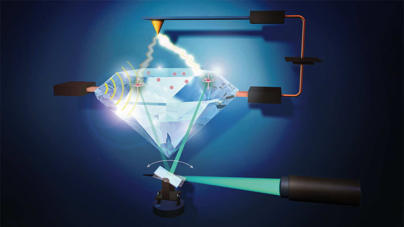
Diamonds with certain optically active defects can be used as highly sensitive sensors or qubits for quantum computers, where the quantum information is stored in the electron spin state of these colour centres. However, the spin states have to be read out optically, which is often experimentally complex. Now, a team at HZB has developed an elegant method using a photo voltage to detect the individual and local spin states of these defects. This could lead to a much more compact design of quantum sensors.

Defects in solids are often undesirable, but they can also provide wonderful new opportunities, for example in diamonds: Here, nitrogen vacancy centres (NV centres) can be introduced whose spin states can be manipulated with microwaves. The information from a single spin can then be read out using light. This makes NV-doped diamonds suitable not only as highly sensitive sensors, but also as qubits for quantum computers.

Up to now: optical detection

However, to determine the state of each individual spin, the photons emitted from the colour centre (carrying the spin) must be measured. Since only single photons are emitted when spins flip, this signal is very weak, leading to a complex experimental set-up for the detection.

Now: photovoltage measured by KPFM

A team at HZB has now presented a novel method to solve this problem. ‘The idea was that such defect centres not only possess a spin state, but also electrical charge,’ says Dr Boris Naydenov. To probe these charges, they modified a variant of atomic force microscopy known as Kelvin probe force microscopy (KPFM): in this process, a laser excites the NV centres, generating free charge carriers that are captured by surface states and thus produce a measurable voltage around an NV centre.

Capturing spin dynamics

‘The photovoltage depends on the electron spin state of the NV centre, and so we can actually read out the individual spin,' says Sergei Trofimov, who carried out the measurements as part of his PhD project. Moreover, with the new method, it is even possible to capture the spin dynamics by coherently manipulating the spin states using microwave excitation.

Outlook: tiny diamond based devices

‘This would open the way to the development of really tiny and compact diamond-based devices, since all that is needed are suitable contacts instead of complex microscopic optics and single-photon detectors,’ says Prof. Klaus Lips, head of the Spins in Energy Conversion and Quantum Information Science department. ‘The newly developed readout method could also be used in other solid-state physics systems where electron spin resonance of spin defects has been observed,’ Lips estimates.

Publication:

Nature communications (2025): Voltage detected single spin dynamics in diamond at ambient conditions
Sergei Trofimov, Klaus Lips, and Boris Naydenov
DOI: 10.1038/s41467-025-58635-3

Contact:

Helmholtz-Zentrum Berlin für Materialien und Energie
Department Spins in Energy Conversion and Quantum Information Science

Dr. Boris Naydenov
+49 30 8062-13116
boris.naydenov(at)helmholtz-berlin.de

Prof. Dr. Klaus Lips
+49 30 8062-14960
lips(at)helmholtz-berlin.de

Dr. Antonia Rötger
Press Officer
+49 30 8062-43733
antonia.roetger(at)helmholtz-berlin.de


Press release HZB, 14 April 2025

Analytics Research Microsystems / Materials Photonics / Optics

Related News

Michele Segantini demonstrates the compact size and the portability of one of the EPRoC-Sensor with a permanent magnet. © Luca Segantini

SpinMagIC: 'EPR on a chip' ensures quality of olive oil and beer

HZB spin-off develops sensor to detect free radicals in food

Related Institutions

  • Helmholtz-Zentrum Berlin für Materialien und Energie GmbH, Elektronenspeicherring BESSY II
  • LinkedInshare0
  • Facebookshare0
  • WhatsAppshare0
  • E-Mail

The development of the Science and Technology Park Berlin Adlershof was and is co-financed by the European Union namely by EFRE. This concerns infrastructure development like construction of technology centres. Furthermore EFRE is used for international projects.

  • © WISTA Management GmbH
  • Legal Notice
  • Privacy Policy
  • Social Media Guide
  • FAQ
  • Contact
  • Press
  • Newsletter
  • RSS
  • International
Member of:
Zukunftsort Adlershof Logo