• Skip to Management
  • Skip to Main menu
  • Skip to Page content
Adlershof Logo
  • WISTA
  • WISTA.Plan
  • WISTA.Service
WISTA direkt
Search
  • de
  • en
  • Adlershof Logo
  • About / Directory
    • Companies / Institutes
    • Science City in numbers
    • Direction / Maps
      • Bus / Train
      • By Car
      • Bicycle
      • Orientation / Maps
      • Trail of Thoughts
  • Newsroom
    • Overview
    • News
      • Social Media Stream
      • Success Stories
    • Events / Calendar
      • Adlershof Dissertation Award
      • Adlershof Research Forum
      • Long Night of Sciences Berlin
    • Adlershof Journal
    • Hot Topics
      • Adlershof Mission "Grand Challenges"
      • Circular Economy
      • Digital infra­structure / 5G campus network
    • Photos / Flyer / Downloads
      • Magazine archive
    • WISTA-Editorial Staff
  • Science / Technology
    • Overview
    • Technology Centres
      • Photonics / Optics
      • Biotech­nology / Envi­ron­ment
      • Micro­systems / Materi­als
      • IT / Media
      • Renewable Energy / Photovoltaics
    • Non-university Research
    • Universities / Colleges
      • Humboldt-Universität zu Berlin
      • Services for Students
    • Young Talents / STEM / School Labs
    • Start-Ups
      • Adlershof Start-Up Centre IGZ
      • Adlershof Founder’s Lab
    • Networks / Management
      • Campus Club Adlershof
  • TV / Media
    • TV and Movie Production
    • Media Services / Companies
    • News and Events
    • Filming Locations
    • Costume Hire
    • GDR Film Archive
    • Tickets / Booking
  • Properties
    • Overview
    • Real Estate Rent
      • Office Space / Workspace / Laboratories
    • Real Estate Offers
      • Commercial Properties
    • ST3AM Working Environments / Coworking
    • Residential
    • Construction
      • Building Projects
      • Architecture
      • Webcam
  • Service
    • Overview
    • Gastronomy / Sport / Culture / Shopping
    • Jobs / Market
    • Social and Healthcare Facilities
    • WISTA-Business Services
    • Event Services / Guided Tours / Hotels
    • Facility Management
    • Downloads / Photos / Videos
    • Jobs for Refugees
  • Hood
    • Overview
    • History
    • Nature Park
    • Culture
    • Technology Park
    • Digital Tours
  • WISTA
  • WISTA.Plan
  • WISTA.Service
WISTA direkt

News

  • Overview
  • News
  • Events / Calendar
  • Adlershof Journal
  • Hot Topics
  • Photos / Flyer / Downloads
  • WISTA-Editorial Staff
  • Adlershof
  • Newsroom
  • News
19. October 2018

Blue phosphorus - mapped and measured for the first time

HZB team was able to examine samples of blue phosphorus at BESSY II for the first time

Blue Phosphorus HZB
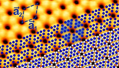
The STM image shows blue phosphorus on a gold substrate. The calculated atomic positions of the slightly elevated P atoms are shown in blue, the lower lying ones in white. Groups of six elevated P atoms appear as triangles. Credit: HZB

Until recently, the existence of "blue" phosphorus was pure theory: Now an HZB team was able to examine samples of blue phosphorus at BESSY II for the first time and confirm via mapping of their electronic band structure that this is actually this exotic phosphorus modification. Blue phosphorus is an interesting candidate for new optoelectronic devices. The results have been published in Nano Letters.

The element phosphorus can exist in  various allotropes and changes its properties with each new form. So far, red, violet, white and black phosphorus have been known. While some phosphorus compounds are essential for life, white phosphorus is poisonous and inflammable and black phosphorus - on the contrary - particularly robust. Now, another allotrope has been identified: In 2014, a team from Michigan State University, USA, performed model calculations to predict that "blue phosphorus" should be also stable. In this form, the phosphorus atoms arrange in a honeycomb structure similar to graphene, however, not completely flat but regularly "buckled". Model calculations showed that blue phosphorus is not a narrow gap semiconductor like black phosphorus in the bulk but possesses the properties of a semiconductor with a rather large band gap of 2 electron volts. This large gap, which is seven times larger than in bulk black phosphorus, is important for optoelectronic applications.

Blue P examined at BESSY II

In 2016, blue phosphorus was successfully stabilized on a gold substrate by evaporation. Nevertheless, only now we know for certain that the resulting material is indeed blue phosphorus. To this end, a team from HZB around Evangelos Golias has probed the electronic band structure of the material at BESSY II. They were able to measure by angle-resolved photoelectron spectroscopy the distribution of electrons in its valence band, setting the lower limit for the band gap of blue phosphorus.

Band structure influenced by the substrate

They found that the P atoms do not arrange independently of the gold substrate but try to adjust to the spacings of the Au atoms. This distorts the corrugated honeycomb lattice in a regular manner which in turn affects the behavior of electrons in blue phosphorus. As a result, the top of the valence band that defines the one end of the semiconducting band gap agrees with the theoretical predictions, but is somewhat shifted.

Outlook: optoelectronic applications

"So far, researchers have mainly used bulk black phosphorus to exfoliate atomically thin layers", Prof. Oliver Rader, head of HZB-Department Materials for green spintronics explains. "These also show a large semiconducting band gap but do not possess the honeycomb structure of blue phosphorus and, above all, cannot be grown directly on a substrate. Our work not only reveals all the material properties of this novel two-dimensional phosphorus allotrope but highlights the impact of the supporting substrate on the behavior of electrons in blue phosphorus, an essential parameter for any optoelectronic application."

Published in Nano Letters (2018): Band renormalization of blue phosphorus on Au(111); E. Golias, M. Krivenkov, A. Varykhalov, J. Sanchez-Barriga and O. Rader

DOI:10.1021/acs.nanolett.8b01305


Contact:

Dr. Evangelos Gkolias
Tel (030) 8062-15695
evangelos.gkolias(at)helmholtz-berlin.de

apl. Prof. Dr. Oliver Rader
Tel (030) 8062-12950
rader(at)helmholtz-berlin.de

Pressestelle:
Dr. Antonia Rötger
Tel (030) 8062-43733
antonia.roetger(at)helmholtz-berlin.de
Renewable Energies Research

Related News

  • two-layer graphene bandstructure. Credit: HZB

    Graphene on the way to superconductivity

    Scientists at HZB have found evidence that double layers of graphene have a property that may let them conduct current completely without resistance
  • Credit: P. Knittel/Fraunhofer IAF

    Nanodiamonds as photocatalysts

    Research team is testing materials for the production of solar fuels at HZB
  • New magnetic splitting effect detected at BESSY II

    Research group observes the formation of Fermi arcs due to magnetic splitting in an antiferromagnet
  • Electronic structure of Sb © HZB/Nature Communication Physics (2021)

    Topological materials for ultrafast spintronics

    New insights into the ultrafast response of topological states of matter to femtosecond laser excitation
1 / 4
  • LinkedInshare0
  • Facebookshare0
  • WhatsAppshare0
  • E-Mail

The development of the Science and Technology Park Berlin Adlershof was and is co-financed by the European Union namely by EFRE. This concerns infrastructure development like construction of technology centres. Furthermore EFRE is used for international projects.

  • © WISTA Management GmbH
  • Legal Notice
  • Privacy Policy
  • Social Media Guide
  • FAQ
  • Contact
  • Press
  • Newsletter
  • RSS
  • International
Member of:
Zukunftsort Adlershof Logo