• Skip to Management
  • Skip to Main menu
  • Skip to Page content
Adlershof Logo
  • WISTA
  • WISTA.Plan
  • WISTA.Service
WISTA direkt
Search
  • de
  • en
  • Adlershof Logo
  • About / Directory
    • Companies / Institutes
    • Science City in numbers
    • Direction / Maps
      • Bus / Train
      • By Car
      • Bicycle
      • Orientation / Maps
      • Trail of Thoughts
  • Newsroom
    • Overview
    • News
      • Social Media Stream
      • Success Stories
    • Events / Calendar
      • Adlershof Dissertation Award
      • Adlershof Research Forum
      • Long Night of Sciences Berlin
    • Adlershof Journal
    • Hot Topics
      • Adlershof Mission "Grand Challenges"
      • Circular Economy
      • Digital infra­structure / 5G campus network
    • Photos / Flyer / Downloads
      • Magazine archive
    • WISTA-Editorial Staff
  • Science / Technology
    • Overview
    • Technology Centres
      • Photonics / Optics
      • Biotech­nology / Envi­ron­ment
      • Micro­systems / Materi­als
      • IT / Media
      • Renewable Energy / Photovoltaics
    • Non-university Research
    • Universities / Colleges
      • Humboldt-Universität zu Berlin
      • Services for Students
    • Young Talents / STEM / School Labs
    • Start-Ups
      • Adlershof Start-Up Centre IGZ
      • Adlershof Founder’s Lab
    • Networks / Management
      • Campus Club Adlershof
  • TV / Media
    • TV and Movie Production
    • Media Services / Companies
    • News and Events
    • Filming Locations
    • Costume Hire
    • GDR Film Archive
    • Tickets / Booking
  • Properties
    • Overview
    • Real Estate Rent
      • Office Space / Workspace / Laboratories
    • Real Estate Offers
      • Commercial Properties
    • ST3AM Working Environments / Coworking
    • Residential
    • Construction
      • Building Projects
      • Architecture
      • Webcam
  • Service
    • Overview
    • Gastronomy / Sport / Culture / Shopping
    • Jobs / Market
    • Social and Healthcare Facilities
    • WISTA-Business Services
    • Event Services / Guided Tours / Hotels
    • Facility Management
    • Downloads / Photos / Videos
    • Jobs for Refugees
  • Hood
    • Overview
    • History
    • Nature Park
    • Culture
    • Technology Park
    • Digital Tours
  • WISTA
  • WISTA.Plan
  • WISTA.Service
WISTA direkt

News

  • Overview
  • News
  • Events / Calendar
  • Adlershof Journal
  • Hot Topics
  • Photos / Flyer / Downloads
  • WISTA-Editorial Staff
  • Adlershof
  • Newsroom
  • News
25. March 2014

Buried layers, hidden treasures

Adlershof’s ingenious strategies of analysis for solar cells and mine deposits

The new Energy Materials In-Situ Laboratory Berlin (EMIL) will start operating in 2015

The inside of a solar cell contains areas in which the desired charge transport might be blocked. Prof. Klaus Lips from the Helmholtz-Centre Berlin (HZB), who teaches ”Analytics for Photovoltaics“ at the FU Berlin, calls it a ”buried layer“. ”This is the boundary layer between the lightactive layer, usually made of crystalline silica, and the charge-separating interface,“ says the head of the project Energy Materials In-Situ Laboratory Berlin (EMIL) which the HZB and the Max-Planck-Society (MPG) are involved in. At that point, losses can occur that impair efficiency.

New materials are in demand. Production, for example the growth of the light-active layer, often requires ultrahigh vacuum and highest purity. During the subsequent analysis using X-ray beamlines, for instance in the electron storage ring BESSY II, this is currently not possible. When transferring the sample into the X-ray tube, interfering dust particles or gas molecules cling to it.

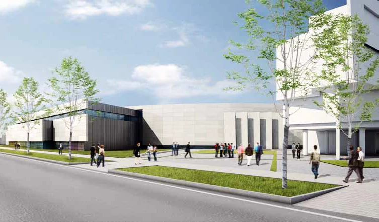
This is due to change with EMIL, a worldwide unique sample preparation and analysis laboratory, which will be docked to BESSY II. ”As of 2015, we can transfer the samples directly into the X-ray spectrometer without having to remove them from the ultra-high vacuum,“ says Lips. Processes occurring on the sensitive boundary layers of the photovoltaic modules can thus be analysed already during production. It would also be possible to observe catalysts at work using this method. Private companies will be able to use the facility.

The industry may also be interested in the projects that are currently being coordinated in Adlershof by the Institute for Scientific Instruments (IfG) with substantial support by the Institute for Applied Photonics (IAP). They deal with on-site analysis of metallic materials. These include the rare-earth metals high-tech devices depend on. Whether exploitation is economically viable can only be determined by detailed on-site analysis. Corresponding tests are carried out using mobile X-ray fluorescence spectrometers that are specifically adapted to the requirements of mining. Combining these with X-ray diffractometry would significantly extend their range of application.

The analyses provided by the XRF-mine-spectrometer that is being developed in the context of the MEGA-project are superfast, precise and, what is more, rich in colour. This Xray colour camera shall be able to analyse even minuscule traces of metallic materials. ”The distribution of elements in the sample is displayed in pseudo-colour,“ says Wedell.

By Paul Janositz for Adlershof Special
www.iap-adlershof.de
www.helmholtz-berlin.de

  • LinkedInshare0
  • Facebookshare0
  • WhatsAppshare0
  • E-Mail

The development of the Science and Technology Park Berlin Adlershof was and is co-financed by the European Union namely by EFRE. This concerns infrastructure development like construction of technology centres. Furthermore EFRE is used for international projects.

  • © WISTA Management GmbH
  • Legal Notice
  • Privacy Policy
  • Social Media Guide
  • FAQ
  • Contact
  • Press
  • Newsletter
  • RSS
  • International
Member of:
Zukunftsort Adlershof Logo