• Skip to Management
  • Skip to Main menu
  • Skip to Page content
Adlershof Logo
  • WISTA
  • WISTA.Plan
  • WISTA.Service
WISTA direkt
Search
  • de
  • en
  • Adlershof Logo
  • About / Directory
    • Companies / Institutes
    • Science City in numbers
    • Direction / Maps
      • Bus / Train
      • By Car
      • Bicycle
      • Orientation / Maps
      • Trail of Thoughts
  • Newsroom
    • Overview
    • News
      • Social Media Stream
      • Success Stories
    • Events / Calendar
      • Adlershof Dissertation Award
      • Adlershof Research Forum
      • Long Night of Sciences Berlin
    • Adlershof Journal
    • Hot Topics
      • Adlershof Mission "Grand Challenges"
      • Circular Economy
      • Digital infra­structure / 5G campus network
    • Photos / Flyer / Downloads
      • Magazine archive
    • WISTA-Editorial Staff
  • Science / Technology
    • Overview
    • Technology Centres
      • Photonics / Optics
      • Biotech­nology / Envi­ron­ment
      • Micro­systems / Materi­als
      • IT / Media
      • Renewable Energy / Photovoltaics
    • Non-university Research
    • Universities / Colleges
      • Humboldt-Universität zu Berlin
      • Services for Students
    • Young Talents / STEM / School Labs
    • Start-Ups
      • Adlershof Start-Up Centre IGZ
      • Adlershof Founder’s Lab
    • Networks / Management
      • Campus Club Adlershof
  • TV / Media
    • TV and Movie Production
    • Media Services / Companies
    • News and Events
    • Filming Locations
    • Costume Hire
    • GDR Film Archive
    • Tickets / Booking
  • Properties
    • Overview
    • Real Estate Rent
      • Office Space / Workspace / Laboratories
    • Real Estate Offers
      • Commercial Properties
    • ST3AM Working Environments / Coworking
    • Residential
    • Construction
      • Building Projects
      • Architecture
      • Webcam
  • Service
    • Overview
    • Gastronomy / Sport / Culture / Shopping
    • Jobs / Market
    • Social and Healthcare Facilities
    • WISTA-Business Services
    • Event Services / Guided Tours / Hotels
    • Facility Management
    • Downloads / Photos / Videos
    • Jobs for Refugees
  • Hood
    • Overview
    • History
    • Nature Park
    • Culture
    • Technology Park
    • Digital Tours
  • WISTA
  • WISTA.Plan
  • WISTA.Service
WISTA direkt

News

  • Overview
  • News
  • Events / Calendar
  • Adlershof Journal
  • Hot Topics
  • Photos / Flyer / Downloads
  • WISTA-Editorial Staff
  • Adlershof
  • Newsroom
  • News
22. June 2016

Coexistence of superconductivity and charge density waves observed

Scanning electron microscopy in combination with EELS electron spectroscopy permits to visualise atomic positions of the individual atoms in the heterostructure: Superconducting regions of YBaCuO are identified by yttrium (blue) and copper (pink), the fer
Scanning electron microscopy in combination with EELS electron spectroscopy permits to visualise atomic positions of the individual atoms in the heterostructure: Superconducting regions of YBaCuO are identified by yttrium (blue) and copper (pink), the ferromagnetic layers by manganese (green) and lanthanum (red). Courtesy MPI Stuttgart.

Physicists at BESSY II studied an artificial structure composed of alternating layers of ferromagnetic and superconducting materials. Charge density waves induced by the interfaces were found to extend deeply into the superconducting regions, indicating new ways to manipulate superconductivity. The results are now being published in Nature Materials.

High-Tc superconductors were discovered 30 years ago: A class of ceramic metal oxide materials was found to pass electrical current without energy losses. In contrast to conventional superconductors that have to be cooled almost to absolute zero, this property appears already at comparably high temperatures. In prototypical yttrium barium copper oxide (YBaCuO), the transition temperature is 92 Kelvin (minus 181 degrees centigrade). Hence, liquid nitrogen suffices as coolant to reach the superconducting phase. The discovery of high-temperature superconductivity has started a quest for applications, which are being implemented now. Until now, however, the microscopic mechanism of high-Tc superconductivity is still matter of debate.

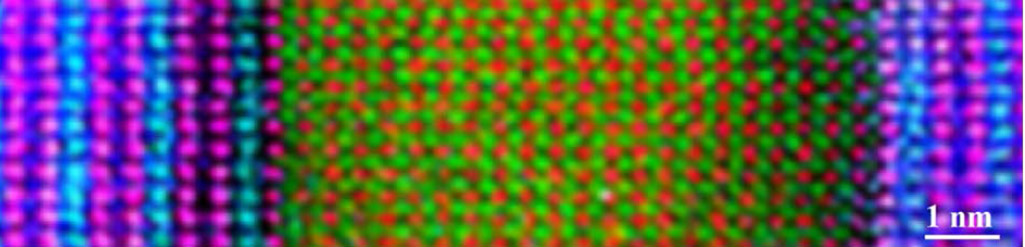
Superconducting and feromagnetic thin layers

A team of scientists lead by Prof. Bernhard Keimer, MPI for Solid State Research, and Dr. Eugen Weschke, HZB, have now investigated an artificial layer system composed of alternating nanolayers of YBaCuO and a ferromagnetic material. The thicknesses of the YBaCuO layers varied between 10 nm and 50 nm.

Tiny collective modulations of valence electrons observed

As interfaces often determine the properties of such heterostructures, physicists were particularly interested in their role for the present system. During his PhD work using resonant x-ray diffraction at BESSY II, Alex Frano could detect tiny collective modulations of valence electrons around Cu atoms in the YBaCuO layer. Data analysis revealed that the resulting charge density wave does not remain located close to the interface but extends across the whole layer. “ This finding is quite a surprise, as previous studies revealed a strong tendency of superconductivity to suppress the formation of charge density waves”, explains Frano.

Charge density wave is stabilized

“Engineering artifical interfaces in heterostructures of ferromagnetic and superconducting layers allowed to stabilize charge density waves even in the presence of superconductivity: YBaCuO remains superconducting, while the charges arrange in a periodic structure”, explains Weschke, “exploring the details of this coexistence on a microscopic scale is a challenging task for future experiments.” A most exciting perspective of the present results is paving the way to controlling the superconducting state itself.

Publication:

Long-range charge-density-wave proximity effect at cuprate/manganate interfaces, A. Frano, S. Blanco-Canosa, E. Schierle, Y. Lu, M. Wu, M. Bluschke, M. Minola, G. Christiani, H. U. Habermeier, G. Logvenov, Y. Wang, P. A. van Aken, E. Benckiser, E. Weschke, M. Le Tacon & B. Keimer, Nature Materials (2016) doi: 10.1038/nmat4682

More Information:

Helmholtz-Zentrum Berlin für Materialien und Energie
Department Quantum Phenomena in Novel Materials

Dr. Eugen Weschke
Tel.: (030) 8062-13409
Fax: (030) 8062-15752
Email: eugen.weschke(at)helmholtz-berlin.de

Dr. Enrico Schierle
Tel.: (030) 8062-15760
Fax: (030) 8062-15752
Email: enrico.schierle(at)helmholtz-berlin.de

  • LinkedInshare0
  • Facebookshare0
  • WhatsAppshare0
  • E-Mail

The development of the Science and Technology Park Berlin Adlershof was and is co-financed by the European Union namely by EFRE. This concerns infrastructure development like construction of technology centres. Furthermore EFRE is used for international projects.

  • © WISTA Management GmbH
  • Legal Notice
  • Privacy Policy
  • Social Media Guide
  • FAQ
  • Contact
  • Press
  • Newsletter
  • RSS
  • International
Member of:
Zukunftsort Adlershof Logo