Detecting fluorescence signals from nanoscale thin films
New measurement technique from INNOVENT e.V. and Ferdinand-Braun-Institut opens up a variety of possibilities in product labeling
Researchers from INNOVENT e.V. and Ferdinand-Braun-Institut gGmbH have developed a measurement technique that allows to detect nanoscale fluorescent thin films for the first time without using expensive laboratory equipment. The addressed fields of application of fluorescent thin films and the associated analysis technology are in areas such as security, logistics and merchandise management.
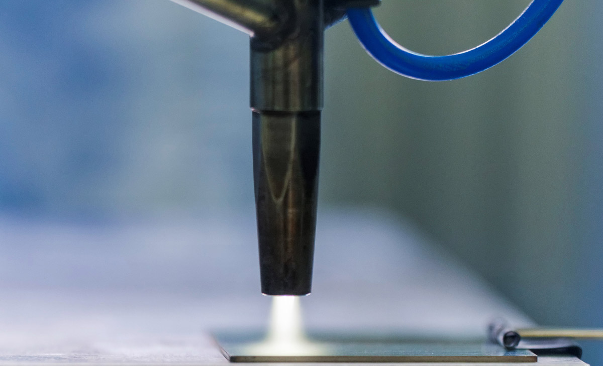
The Jena-based industrial research institution INNOVENT e.V. has incorporated fluorescent nanoparticles into thin-film technologies. These particles can now be detected thanks to a special measurement method developed at the Ferdinand-Braun-Institut (FBH) in Berlin. Till date, this was not possible because the fluorescent materials provide very low intensity signals. The technology is based on plasma and sol-gel coatings. To further develop the patented nano-fluorescence technology so that it can be used commercially with a handheld device and mobile app in the future, additional partners are currently being sought.
The novel coatings can be made invisible to the eye and customized to the respective application. For example, the functionality of the surface can be designed as a barrier layer to prevent metals from corrosion or to make films impermeable to gases. Easy-to-clean layers can also be created in this way, which are equipped with special hydrophilic, hydrophobic or antimicrobial properties. Very low concentrations of the nanoparticles, of less than 0.5 %, need to be introduced into the 200-500 nm thin layers. This guarantees that materials are used economically and ensures that the labeled products are recyclable.
The verification process
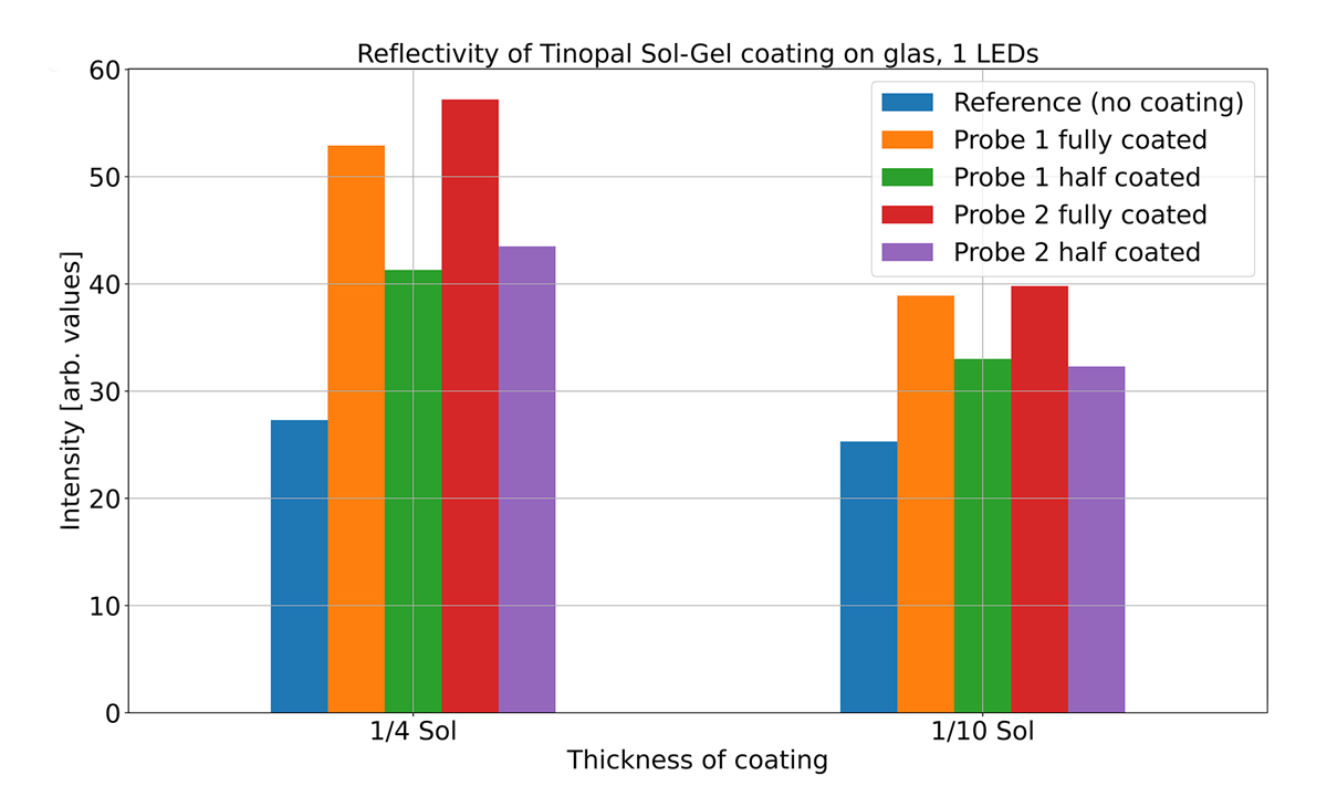
For the high sensitivity detection of the nanoscale fluorescent thin films, the layers are excited using UV light, which is detected by a photodetector with an optical filter. The fluorescence can be measured within a few seconds as successfully demonstrated in a laboratory setup. In the future, such sensitive measurements in many application areas will no longer have to be carried out in the laboratory thanks to the small size of the components. They could be performed directly in production areas, in logistics companies or at customs offices, because the laboratory setup at FBH is so compact that it is also suitable for mobile applications. The detection unit can be constructed as a miniaturized system to identify specific dyes or as a standardized ‘universal system’ with interchangeable LEDs and/or filters.
New possibilities for product labeling
The patented nano-fluorescence technology offers companies that use functional thin-film coatings and label products the opportunity to enter new markets in this area. Coatings can be deposited over small or large areas, depending on the product, and dyes can be used economically. Identifications such as logos or barcodes can be ‘engraved’ by laser into these color-coated surfaces for ‘track & trace’ to track products in logistics. These markings with line widths of a few micrometers can be detected with a handheld fluorescence detection system. The coatings themselves adhere to a variety of materials such as plastics, metals, glass/ceramics, lightweight and 3D printed products.
The markings can also be used in-house for managing semi-finished product logistics and for organizational purposes in supply chains. The technology is equally suitable for product labeling – as a certificate of authenticity for mass-produced items as well as customizable for high-value quality products. Combination or variation of the fluorescent materials and ‘engravings’ can be used to increase flexibility. The patent-protected coatings can also be licensed to interested companies.
Contact:
INNOVENT e. V. Technologienentwicklung Jena
Dr. Sebastian Spange / Dr. Sven Gerullis
Email: SS2(at)innovent-jena.de / SG(at)innovent-jena.de
www.innovent-jena.de
Ferdinand-Braun-Institut gGmbH
Dr. Neysha Lobo Ploch
Email: Neysha.Lobo-Ploch(at)fbh-berlin.de
www.fbh-berlin.de
Press release 29 June 2022