• Skip to Management
  • Skip to Main menu
  • Skip to Page content
Adlershof Logo
  • WISTA
  • WISTA.Plan
  • WISTA.Service
WISTA direkt
Search
  • de
  • en
  • Adlershof Logo
  • About / Directory
    • Companies / Institutes
    • Science City in numbers
    • Direction / Maps
      • Bus / Train
      • By Car
      • Bicycle
      • Orientation / Maps
      • Trail of Thoughts
  • Newsroom
    • Overview
    • News
      • Social Media Stream
      • Success Stories
    • Events / Calendar
      • Long Night of Sciences Berlin
      • Adlershof Dissertation Award
      • Adlershof Research Forum
    • Adlershof Journal
    • Hot Topics
      • Grand Challenges
      • Circular Economy
      • Digital infra­structure / 5G campus network
    • Photos / Flyer / Downloads
      • Magazine archive
    • WISTA-Editorial Staff
  • Science / Technology
    • Overview
    • Technology Centres
      • Photonics / Optics
      • Biotech­nology / Envi­ron­ment
      • Micro­systems / Materi­als
      • IT / Media
      • Renewable Energy / Photovoltaics
    • Non-university Research
    • Universities / Colleges
      • Humboldt-Universität zu Berlin
      • Services for Students
    • Young Talents / STEM / School Labs
    • Start-Ups
      • Adlershof Start-Up Centre IGZ
      • Adlershof Founder’s Lab
    • Networks / Management
      • Campus Club Adlershof
  • TV / Media
    • TV and Movie Production
    • Media Services / Companies
    • News and Events
    • Filming Locations
    • Costume Hire
    • GDR Film Archive
    • Tickets / Booking
  • Properties
    • Overview
    • Real Estate Rent
      • Office Space / Workspace / Laboratories
    • Real Estate Offers
      • Commercial Properties
    • ST3AM Working Environments / Coworking
    • Residential
    • Construction
      • Building Projects
      • Architecture
      • Webcam
  • Service
    • Overview
    • Gastronomy / Sport / Culture / Shopping
    • Jobs / Market
    • Social and Healthcare Facilities
    • WISTA-Business Services
    • Event Services / Guided Tours / Hotels
    • Facility Management
    • Downloads / Photos / Videos
    • Jobs for Refugees
  • Hood
    • Overview
    • History
    • Nature Park
    • Culture
    • Technology Park
    • Digital Tours
  • WISTA
  • WISTA.Plan
  • WISTA.Service
WISTA direkt

News

  • Overview
  • News
  • Events / Calendar
  • Adlershof Journal
  • Hot Topics
  • Photos / Flyer / Downloads
  • WISTA-Editorial Staff
  • Adlershof
  • Newsroom
  • News
02. July 2014

Electrostatics do the trick

A simple model describes what happens between organic semiconductors and metals

When inserting an ultrathin dielectric between metal electrode and organic semiconductor, charge carriers (shown here for a positively charged holes in red) are, counter intuitively, more efficiently extracted from their transport level (blue) in the organic to the Fermi level (black) in the metal than without the interlayer. Image: M Oehzelt/HZB

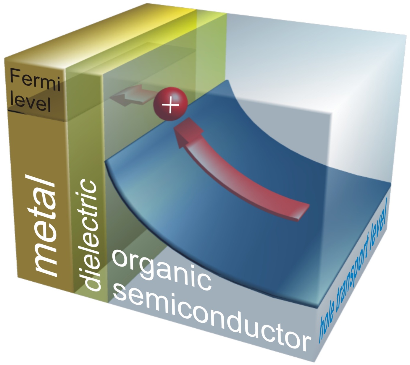
Organic semiconductors allow for flexible displays (OLEDs), solar cells (OPVCs), and other interesting applications. One common problem in these devices, however, is the interface between the metallic contacts and the organic semiconductor material, where undesirable losses occur. Now Dr. Martin Oehzelt has shown what these losses between the metal and the organic semiconductors depend upon and how to minimize them. In particular, his model also explains why a thin, electrically insulating layer between the two materials can even facilitate the transition of charge carriers. His results have recently been published in Nature Communications.

Currently, there are many different approaches describing the interface between organic semiconductor materials and metallic contacts. These somewhat contradictory theories, none of which is universally valid for all cases, have now been unified by Oehzelt and developed into a single coherent model based on the electrostatic potential caused by the charge carriers in the metal and the organic semiconductor. “I calculated the impact of the charge carrier distribution on the electronic states at the interface and how these changes feed back onto the charge carrier distribution”, he explains. Oehzelt is presently conducting research with Dr. Georg Heimel as a postdoc for Prof. Norbert Koch, who works at the Humboldt-Universität zu Berlin and the Helmholtz-Zentrum Berlin.

Such calculations have never been so comprehensively carried out before. Performing them, Oehzelt states: “it was surprising to me that the quantum physical level was not that important. The electrostatic effects predominated! The agreement between our model and the experimental data were astonishing.” On the example of pentacene, a common organic semiconductor, Oehzelt has quantitatively checked the model’s predictions for interface losses.

The energy distribution of the electronic states in organic semiconductors determines the minimum energy barrier the charge carriers have to overcome in transitioning from or into the metal. The calculation demonstrates that the shape of this energy barrier can vary, from a step-function to slow, continuously rising curves that lead to considerably lower losses. The latter can be achieved by introducing an extremely thin insulating layer between the organic semiconductor and the metal. Contrary to the general expectation, the introduction of an insulator thus improves the electrical contact.

The results of this work could notably simplify optimization of interfaces and contacts and, thereby, the development of more efficient organic electronic devices.

The work has recently been published in Nature Communications
doi 10.1038/ncomms5174

More Information:

Helmholtz-Zentrum Berlin für Materialien und Energie
Research Group Molecular Systems
Dr. Martin Oehzelt
Tel.: (030) 8062-15148
E-Mail: martin.oehzelt(at)helmholtz-berlin.de

Press Office:
Dr. Antonia Rötger
Tel.: (030) 8062-43733
Fax: (030) 8062-42998
E-Mail: antonia.roetger(at)helmholtz-berlin.de

www.helmholtz-berlin.de


  • LinkedInshare0
  • Facebookshare0
  • WhatsAppshare0
  • E-Mail

The development of the Science and Technology Park Berlin Adlershof was and is co-financed by the European Union namely by EFRE. This concerns infrastructure development like construction of technology centres. Furthermore EFRE is used for international projects.

  • © WISTA Management GmbH
  • Legal Notice
  • Privacy Policy
  • Social Media Guide
  • FAQ
  • Contact
  • Press
  • Newsletter
  • RSS
  • International
Member of:
Zukunftsort Adlershof Logo