• Skip to Management
  • Skip to Main menu
  • Skip to Page content
Adlershof Logo
  • WISTA
  • WISTA.Plan
  • WISTA.Service
WISTA direkt
Search
  • de
  • en
  • Adlershof Logo
  • About / Directory
    • Companies / Institutes
    • Science City in numbers
    • Direction / Maps
      • Bus / Train
      • By Car
      • Bicycle
      • Orientation / Maps
      • Trail of Thoughts
  • Newsroom
    • Overview
    • News
      • Social Media Stream
      • Success Stories
    • Events / Calendar
      • Adlershof Dissertation Award
      • Adlershof Research Forum
      • Long Night of Sciences Berlin
    • Adlershof Journal
    • Hot Topics
      • Adlershof Mission "Grand Challenges"
      • Circular Economy
      • Digital infra­structure / 5G campus network
    • Photos / Flyer / Downloads
      • Magazine archive
    • WISTA-Editorial Staff
  • Science / Technology
    • Overview
    • Technology Centres
      • Photonics / Optics
      • Biotech­nology / Envi­ron­ment
      • Micro­systems / Materi­als
      • IT / Media
      • Renewable Energy / Photovoltaics
    • Non-university Research
    • Universities / Colleges
      • Humboldt-Universität zu Berlin
      • Services for Students
    • Young Talents / STEM / School Labs
    • Start-Ups
      • Adlershof Start-Up Centre IGZ
      • Adlershof Founder’s Lab
    • Networks / Management
      • Campus Club Adlershof
  • TV / Media
    • TV and Movie Production
    • Media Services / Companies
    • News and Events
    • Filming Locations
    • Costume Hire
    • GDR Film Archive
    • Tickets / Booking
  • Properties
    • Overview
    • Real Estate Rent
      • Office Space / Workspace / Laboratories
    • Real Estate Offers
      • Commercial Properties
    • ST3AM Working Environments / Coworking
    • Residential
    • Construction
      • Building Projects
      • Architecture
      • Webcam
  • Service
    • Overview
    • Gastronomy / Sport / Culture / Shopping
    • Jobs / Market
    • Social and Healthcare Facilities
    • WISTA-Business Services
    • Event Services / Guided Tours / Hotels
    • Facility Management
    • Downloads / Photos / Videos
    • Jobs for Refugees
  • Hood
    • Overview
    • History
    • Nature Park
    • Culture
    • Technology Park
    • Digital Tours
  • WISTA
  • WISTA.Plan
  • WISTA.Service
WISTA direkt

News

  • Overview
  • News
  • Events / Calendar
  • Adlershof Journal
  • Hot Topics
  • Photos / Flyer / Downloads
  • WISTA-Editorial Staff
  • Adlershof
  • Newsroom
  • News
18. July 2018

Flipping the switch on supramolecular electronics

For the first time, two-dimensional materials have been decorated with a photoswitchable molecular layer, and electronic components have been fabricated from the resulting hybrid materials that can be controlled by light

[Translate to English:] Bild: IRIS Adlershof

The results of this fruitful collaboration of several European research groups have been published in Nature Communications.

Owing to their outstanding electrical, optical, chemical and thermal properties, two-dimensional (2D) materials, which consist of a single layer of atoms, hold great potential for technological applications such as electronic devices, sensors, catalysts, energy conversion and storage devices, among others. Thanks to their ultra-high surface sensitivity, 2D materials represent an ideal platform to study the interplay between nanoscale molecular assembly on surfaces and macroscopic electrical transport in devices.

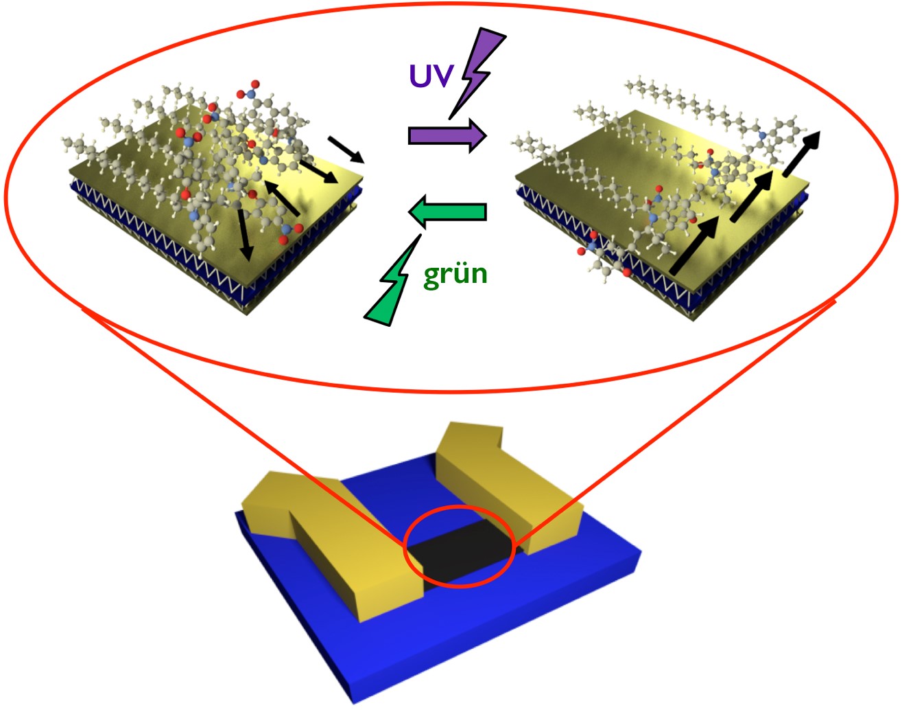
In order to provide a unique light-responsivity to devices, the researchers have designed and synthesized a photoswitchable spiropyran building block, which is equipped with an anchoring group and which can be reversibly interconverted between two different forms by illumination with ultraviolet and visible light, respectively. On the surface of 2D materials, such as graphene or molybdenum disulfide (MoS2), the molecular photoswitches self-assemble into highly ordered ultrathin layers, thereby generating a hybrid, atomically precise superlattice. Upon illumination the system undergoes a collective structural rearrangement, which could be directly visualized and monitored with sub-nanometer resolution by scanning tunneling microscopy. This light-induced reorganization at the molecular level induces an optical modulation of the energetics of the underlying 2D material, which translates into a change in the electrical characteristics of the fabricated hybrid devices. In this regard, the collective nature of self-assembly allows to convert single-molecule events into a spatially homogeneous switching action, which generates a macroscopic electrical response in graphene and MoS2.

"With our versatile approach of molecularly tailoring 2D materials, we are taking supramolecular electronics to a new level and closer to future applications," says Prof. Stefan Hecht, who is researching hybrid materials at IRIS Adlershof. The work is groundbreaking for the realization of multifunctional hybrid components powered by nature's primary energy source - sunlight.


Further Information

Publication

 
“Collective molecular switching in hybrid superlattices for light-modulated two-dimensional electronics”

by: Marco Gobbi, Sara Bonacchi, Jian X. Lian, Alexandre Vercouter, Simone Bertolazzi, Björn Zyska, Melanie Timpel, Roberta Tatti, Yoann Olivier, Stefan Hecht, Marco V. Nardi, David Beljonne, Emanuele Orgiu and Paolo Samorì

in: Nature Communications2018, 9, 2661, DOI: 10.1038/s41467-018-04932-z

  • LinkedInshare0
  • Facebookshare0
  • WhatsAppshare0
  • E-Mail

The development of the Science and Technology Park Berlin Adlershof was and is co-financed by the European Union namely by EFRE. This concerns infrastructure development like construction of technology centres. Furthermore EFRE is used for international projects.

  • © WISTA Management GmbH
  • Legal Notice
  • Privacy Policy
  • Social Media Guide
  • FAQ
  • Contact
  • Press
  • Newsletter
  • RSS
  • International
Member of:
Zukunftsort Adlershof Logo