HZB team analyses mesoporous silicon
The modification of the semiconductor promises great potential for technical applications
Silicon is the best-known semiconductor material. However, controlled nanostructuring drastically alters the material's properties. Using a specially developed etching apparatus, a team at HZB has now produced mesoporous silicon layers with countless tiny pores and investigated their electrical and thermal conductivity. For the first time, the researchers elucidated the electronic transport mechanism in this mesoporous silicon. The material has great potential for applications and could also be used to thermally insulate qubits for quantum computers.
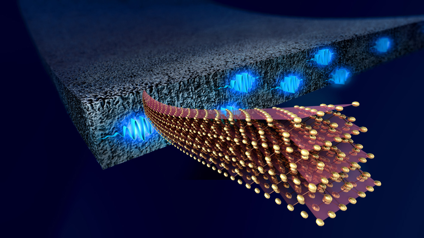
Mesoporous silicon is crystalline silicon with disordered nanometer-sized pores. The material has a huge internal surface area and is also biocompatible. This opens up a wide range of potential applications, from biosensors to battery anodes and capacitors. In addition, the material’s exceptionally low thermal conductivity suggests applications as thermal insulator.
Understanding transport properties in silicon nanostructures
Although mesoporous silicon has been known for decades, until now there has been a lack of fundamental understanding of the transport of charge carriers and the possible involvement of lattice vibrations (phonons). ‘However, in order to develop the material in a targeted manner, a precise understanding of the transport properties and processes is required,’ says Priv. Doz. Dr. Klaus Habicht, who heads the Dynamics and Transport in Quantum Materials (QM-ADT) department at HZB.
Habicht and his team have now presented new insights. They synthesised a series of silicon nanostructures using an etching technique optimised at HZB and determined the temperature-dependent electrical conductivity and thermopower.
Electrons in wavelike states dominate the transport
‘By analysing the data, we were able to unambiguously identify the fundamental charge transport process,’ says Dr. Tommy Hofmann, first author of the study. The key finding: ‘It is not the electrons, localised by disorder, that hop from one localised state to the next that dominate charge transport, but those in extended, wave-like states.’ In this case, the conductivity decreases with increasing disorder. The activation energy required to move charge carriers over a disorder-dependent ‘mobility edge’ increases.
In contrast to a hopping process, lattice vibrations do not play a role in charge transport. This was particularly evident from measurements of the Seebeck effect, which probe the electrical voltage across a sample when it is exposed to a temperature difference along a defined direction.
‘This is the first time that we have provided a reliable and novel explanation for the microscopic charge carrier transport in disordered, nanostructured silicon,’ says Dr. Tommy Hofmann.
Manifold applications
These results are highly relevant to practical applications, as mesoporous silicon could be ideal for silicon-based qubits. These qubits operate at cryogenic temperatures, typically below 1 Kelvin, and require very good thermal insulation to prevent heat from the surrounding environment from being absorbed and erasing the information stored in the qubits. ‘To use a metaphor, you could think of mesoporous silicon as a type of insulating foam used in building construction,’ says Habicht.
The use of mesoporous silicon may also be suitable for semiconductor applications that have so far failed due to the high thermal conductivity of crystalline or polycrystalline silicon. ‘The disorder can be used in a targeted way,’ says Habicht. Semiconductors with purely randomly distributed mesopores would be an exciting new class of materials for technical applications ranging from photovoltaics, thermal management and nanoelectronics to qubits for quantum computers.
Publication:
Small Structures (2025): Electrons, Localization but no Hopping: Disorder as Key for Understanding Charge Transport in Mesoporous Silicon
Tommy Hofmann, Haider Haseeb, Danny Kojda, Natalia Gostkowska-Lekner, Klaus Habicht
https://onlinelibrary.wiley.com/doi/10.1002/sstr.202400437
Contact:
Helmholtz-Zentrum Berlin für Materialien und Energie
Department Dynamics and Transport in Quantum Materials
Dr. habil. Tommy Hofmann
+49 30 8062-42780
tommy.hofmann(at)helmholtz-berlin.de
Priv.-Doz. Dr. Klaus Habicht
+49 30 8062-42807
habicht(at)helmholtz-berlin.de
Press Officer:
Dr. Antonia Rötger
+49 30 8062-43733
antonia.roetger(at)helmholtz-berlin.de
Press release HZB, 25 February 2025