• Skip to Management
  • Skip to Main menu
  • Skip to Page content
Adlershof Logo
  • WISTA
  • WISTA.Plan
  • WISTA.Service
WISTA direkt
Search
  • de
  • en
  • Adlershof Logo
  • About / Directory
    • Companies / Institutes
    • Science City in numbers
    • Direction / Maps
      • Bus / Train
      • By Car
      • Bicycle
      • Orientation / Maps
      • Trail of Thoughts
  • Newsroom
    • Overview
    • News
      • Social Media Stream
      • Success Stories
    • Events / Calendar
      • Adlershof Dissertation Award
      • Adlershof Research Forum
      • Long Night of Sciences Berlin
    • Adlershof Journal
    • Hot Topics
      • Adlershof Mission "Grand Challenges"
      • Circular Economy
      • Digital infra­structure / 5G campus network
    • Photos / Flyer / Downloads
      • Magazine archive
    • WISTA-Editorial Staff
  • Science / Technology
    • Overview
    • Technology Centres
      • Photonics / Optics
      • Biotech­nology / Envi­ron­ment
      • Micro­systems / Materi­als
      • IT / Media
      • Renewable Energy / Photovoltaics
    • Non-university Research
    • Universities / Colleges
      • Humboldt-Universität zu Berlin
      • Services for Students
    • Young Talents / STEM / School Labs
    • Start-Ups
      • Adlershof Start-Up Centre IGZ
      • Adlershof Founder’s Lab
    • Networks / Management
      • Campus Club Adlershof
  • TV / Media
    • TV and Movie Production
    • Media Services / Companies
    • News and Events
    • Filming Locations
    • Costume Hire
    • GDR Film Archive
    • Tickets / Booking
  • Properties
    • Overview
    • Real Estate Rent
      • Office Space / Workspace / Laboratories
    • Real Estate Offers
      • Commercial Properties
    • ST3AM Working Environments / Coworking
    • Residential
    • Construction
      • Building Projects
      • Architecture
      • Webcam
  • Service
    • Overview
    • Gastronomy / Sport / Culture / Shopping
    • Jobs / Market
    • Social and Healthcare Facilities
    • WISTA-Business Services
    • Event Services / Guided Tours / Hotels
    • Facility Management
    • Downloads / Photos / Videos
    • Jobs for Refugees
  • Hood
    • Overview
    • History
    • Nature Park
    • Culture
    • Technology Park
    • Digital Tours
  • WISTA
  • WISTA.Plan
  • WISTA.Service
WISTA direkt

News

  • Overview
  • News
  • Events / Calendar
  • Adlershof Journal
  • Hot Topics
  • Photos / Flyer / Downloads
  • WISTA-Editorial Staff
  • Adlershof
  • Newsroom
  • News
12. January 2010

Instruments for the microcosm

Fully automated etching-cluster with high flow capacity for industrial manufacturing

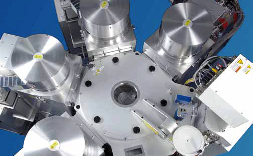
Long trenches and a chessboard of gentle hills stretch to the horizon, broken by vertical shafts that seem to be bottomless. Yet nobody will ever set foot on these bizarre landscapes, the work of developers at Sentech Instruments GmbH in Adlershof.

They are only a few microns across and serve as optical conductors,
tiny lenses, electronic transistors or micromachine componentry. “We not only supply the instruments that can make these structures,” said Dr Albrecht Krüger, one of the two company founders, “we also make the corresponding measuring equipment for research and for monitoring series production, e.g. of solar cells and electronic componentry.”

In order to generate fine structures in the micron and submicron range the experts at Sentech make use of so called reactive ion etching. This involves shooting a sample with a beam of charged gas atoms. The bombardment weakens the chemical bonds between the atoms on the surface. Then they can react with the gas atoms and so be removed from the surface. “With the aid of special ion sources we can generate a very soft, but dense gas beam,” explained Albrecht Krüger. “We can therefore generate clean structures even on the smallest scale.” More detailed investigations into the properties of such tiny forms often make use of polarised light. Oscillating in a precisely defined plane this light impinges on the sample and changes its oscillating plane depending on the consistency of the surface. Measuring this change in the light reflected from the sample provides information on its surface structure.

“On samples that reflect light well this is not a problem,” explained Krüger. Solar cells though are supposed to absorb as much sunlight as possible and reflect only very little. With highly complex measuring technology and mathematical methods for analysing the data Sentech has succeeded in developing a method unrivalled in precision. “We sell more than fifty of these devices every year, and virtually every maker of silicon solar cells has one of our measuring devices,” reported Krüger.

That the work was worth the effort is made clear by the company’s turnover, which grew by 50% in the last two years – and not least of all the move to a three storey production and office building with 2,600 square metres, only a stone’s throw away from the present rented rooms at the Photonics and Optics Centre in Adlershof: the company’s first own head office since it was set up in 1990.

Wolfgang Richter

Link: www.sentech.de

  • LinkedInshare0
  • Facebookshare0
  • WhatsAppshare0
  • E-Mail

The development of the Science and Technology Park Berlin Adlershof was and is co-financed by the European Union namely by EFRE. This concerns infrastructure development like construction of technology centres. Furthermore EFRE is used for international projects.

  • © WISTA Management GmbH
  • Legal Notice
  • Privacy Policy
  • Social Media Guide
  • FAQ
  • Contact
  • Press
  • Newsletter
  • RSS
  • International
Member of:
Zukunftsort Adlershof Logo