Is there electrical current in an insulator?
MBI researchers visualize the transfer of electrons in an insulator
The MBI femtosecond x-ray team (project 3.3) observed an extremely fast transfer of electrons between neighboring atoms by applying a strong optical field to an insulator crystal and mapping its real-space electron distribution with x-rays.
When you first learned about electric currents, any substance, in particular solids, was classified either as a metal or as an insulator. When a battery is attached to a piece of metal, the electrons fly across it going from the negative to the positive terminal, i.e., an electrical current is induced by the voltage. In contrast, applying the same battery to a piece of insulating material one observes essentially zero current. Thus, one might ask, whether the electrons in an insulator do move at all when exposed to a strong electric field (voltage). And, if they move, how fast and how far do they get?
To answer this fundamental question, one needs to measure the position of electrons in the material with a precision of the order of 0.1 nm (0.1 nm=10-10m), roughly corresponding to the distance between neighboring atoms. This is possible by imaging the material with x-rays which are scattered from the electrons and provide their spatial arrangement. In addition, one needs to apply an electric field sufficiently high to move the electrons away from the atoms to which they are bound initially. Such a high field can be provided for a very short time interval of 50 fs (10-15 s) by a strong optical pulse which is sent onto the material.
In the current issue of Physical Review Letters (PRL 109, 147402, 2012), Johannes Stingl, Flavio Zamponi, Benjamin Freyer, Michael Woerner, Thomas Elsaesser and Andreas Borgschulte report the first in-situ x-ray imaging of electron and atom motions induced by a strong optical field. For the ionic prototype material LiBH4, they have determined time-dependent 'electron maps' from x-ray snapshots taken with 100 fs long hard x-ray flashes. Taking x-ray snapshots at various times during and after the optical pulse that provides the electric field, creates a molecular movie of electron and atom motions.
It was a big surprise for the researchers that during the temporal overlap of the optical pulse and the x-ray flash an extremely fast transfer of an electron from the BH4- to the neighboring Li+ ions occurs over a distance of 0.25 nm. Since the electric field of the optical pulse reverses its direction every 1.3 fs, the electron is driven back and forth between the two sites with an extremely high speed of approximately one percent of the speed of light (c = 300.000 km / s). After the optical pulse, the electron returns to the BH4- ion and the original electron distribution is restored. Beyond this quasi-instantaneous reversible electron transfer there is no macroscopic electric current, i.e., the material behaves as an insulator. The large elongation of electrons between neighboring sites makes a strong contribution to the optical properties of LiBH4, the so-called optical polarization.
A quantitative analysis of the electron maps in terms of polarization allows for identifying the electron transfer as the major source of the strong optical polarization which has been observed in all-optical experiments and displays pronounced nonlinearities at high optical fields. Beyond the new insight into fundamental electric and optical properties of insulators, the present experiments suggest applications of LiBH4 and similar ionic insulators for characterizing the temporal structure of hard x-ray pulses by cross-correlating them with ultrashort optical pulses.
Movie:
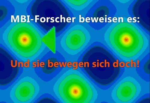
The attached cartoon of the electron motion between neighboring atoms in the LiBH4 crystal. The red curve in the upper panel shows the electric field of the laser pulse as a function of time. The moving blue circle indicates the strength and direction of the electric field of the corresponding frame in the lower panel. The latter shows schematically the electron density in the unit cell of the LiBH4 crystal.
Without the electric field of the laser the electron density on the BH4- anions (brighter spots) is much higher than that on the Li+ cations (darker spots). During the laser pulse the oscillatory electric field of the laser causes strong electron currents between BH4- and Li+ units as indicated by the intensity of the occurring arrows.
Contact:
Michael Woerner, Tel: +49 (0)30 / 6392-1470, email: woerner(at)mbi-berlin.de
Flavio Zamponi, Tel: +49 (0)30 / 6392-1472, email: zamponi(at)mbi-berlin.de
Thomas Elsaesser, Tel.: +49 (0)30 / 6392-1400, email: elsasser(at)mbi-berlin.de
Forschungsverbund Berlin e. V.
Rudower Chaussee 17
12489 Berlin
Tel.: 030 / 6392-3330
email: info(at)fv-berlin.de
www.fv-berlin.de
