Optimised transistors: creating a metal with laser light
Researchers from the Fritz Haber Institute of the Max Planck Society and the Humboldt-Universität zu Berlin make discovery that could increase computing power
From smartphones to computer processors – much of the technology we nowadays use heavily features transistors. They connect many of the different materials that make up these devices, and are essential for any kind of data processing. Because they are so important, scientists and engineers have long tried to optimize them by modifying their material properties, so that they can be used more flexibly. Now, a team of researchers the Fritz Haber Institute of the Max Planck Society and the Humboldt-Universität zu Berlin has found an important clue on how to achieve that.
Transistors are often made up of semiconductors, i.e. materials that conduct electricity, but not quite as well as metals. In common transistors, several semiconductors are combined to control an electrical current. Unfortunately, this limits the performance and size of the device they are built in to. “Basically, it would be ideal to have just one material that can do it all, whenever you need it”, says Prof. Julia Stähler from Humboldt Universität zu Berlin, who led the study at the Fritz Haber Institute. Though the conductivity of semiconductors can be altered by a chemical process called „doping“, this technique, in which atoms of the semiconductor are replaced with other atoms, has limitations. The properties of a material can be changed, but will permanently remain so, while what is actually needed is a material that can switch between different properties. Julia Stähler’s group has found an answer to this question: light.
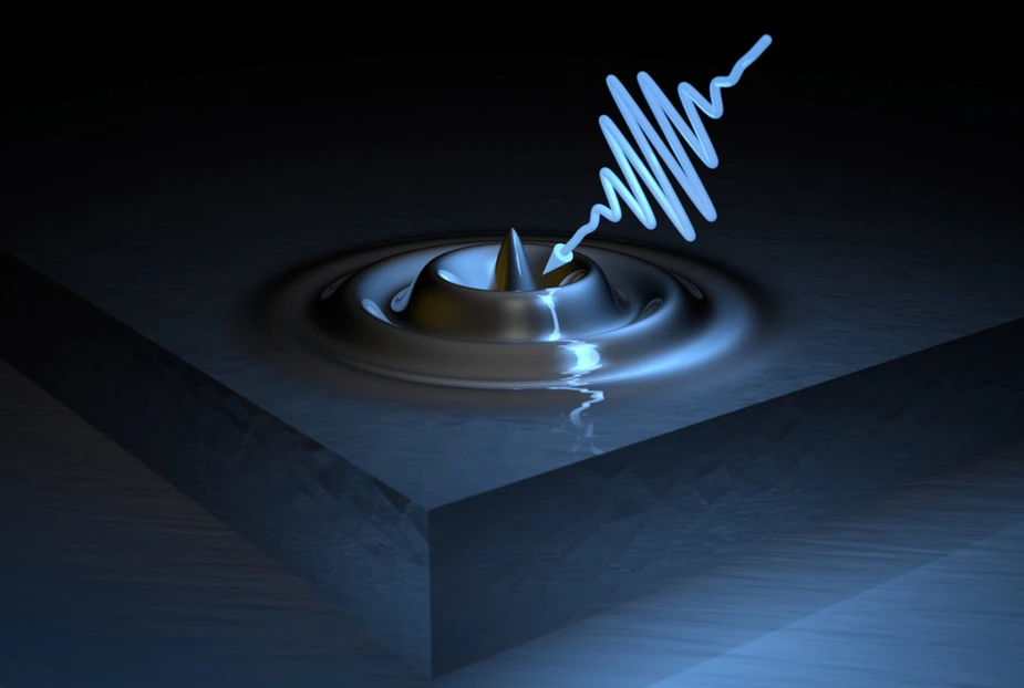
The scientists involved in this study have investigated the popular semiconductor zinc oxide and figured out that by hitting it with a laser, simply illuminating it, the semiconductor surface can be turned into a metal – and back again. This “photo-doping” is achieved by photoexcitation: the light modifies the electronic properties such that electrons suddenly move freely and an electrical current can flow, as it would in metal. Once the light is switched back off, the material also quickly goes back to being a semiconductor. “This mechanism is a completely new and surprising discovery,” says Lukas Gierster, lead author and PhD student in Stähler’s group. “Three things in particular have surprised us: for one, that photo- and chemical doping behave so much alike despite being fundamentally different mechanisms; two, that gigantic changes can be reached with very low laser power; and three, that switching the metal on and off happens so quickly.” The conversion to a metal only takes 20 femtoseconds, i.e. 20 millionth of a billionth of a second. The speed of the re-formation of the semiconductor was especially astonishing as it was orders of magnitude faster than in previous studies. In other words, zinc oxide is an ultrafast switch that has the ‘force’ to “do it all”.
This discovery could be highly beneficial for high-frequency device applications and ultrafast optically controlled transistors by increasing processing speed and simplifying device design. “Our gadgets could become faster – and thus smarter”, Julia Stähler says and adds: “Low-power, ultrafast switching of conduction properties will provide us with high speed and design flexibility.” She and her group are convinced that the same will prove true for other semiconducting materials, so that their discovery will likely reach much further than just zinc oxide.
Further information:
Publication: dx.doi.org/10.1038/s41467-021-21203-6
Teaser video: youtu.be/iuGmfRFA6aY
Contact:
Prof. Dr. Julia Stähler
Department of Chemistry
Humboldt-Universität zu Berlin
Email: julia.staehler(at)hu-berlin.de
www.electrondynamix.de
Press release HU, 12 February 2021
