• Skip to Management
  • Skip to Main menu
  • Skip to Page content
Adlershof Logo
  • WISTA
  • WISTA.Plan
  • WISTA.Service
WISTA direkt
Search
  • de
  • en
  • Adlershof Logo
  • About / Directory
    • Companies / Institutes
    • Science City in numbers
    • Direction / Maps
      • Bus / Train
      • By Car
      • Bicycle
      • Orientation / Maps
      • Trail of Thoughts
  • Newsroom
    • Overview
    • News
      • Social Media Stream
      • Success Stories
    • Events / Calendar
      • Adlershof Dissertation Award
      • Adlershof Research Forum
      • Long Night of Sciences Berlin
    • Adlershof Journal
    • Hot Topics
      • Adlershof Mission "Grand Challenges"
      • Circular Economy
      • Digital infra­structure / 5G campus network
    • Photos / Flyer / Downloads
      • Magazine archive
    • WISTA-Editorial Staff
  • Science / Technology
    • Overview
    • Technology Centres
      • Photonics / Optics
      • Biotech­nology / Envi­ron­ment
      • Micro­systems / Materi­als
      • IT / Media
      • Renewable Energy / Photovoltaics
    • Non-university Research
    • Universities / Colleges
      • Humboldt-Universität zu Berlin
      • Services for Students
    • Young Talents / STEM / School Labs
    • Start-Ups
      • Adlershof Start-Up Centre IGZ
      • Adlershof Founder’s Lab
    • Networks / Management
      • Campus Club Adlershof
  • TV / Media
    • TV and Movie Production
    • Media Services / Companies
    • News and Events
    • Filming Locations
    • Costume Hire
    • GDR Film Archive
    • Tickets / Booking
  • Properties
    • Overview
    • Real Estate Rent
      • Office Space / Workspace / Laboratories
    • Real Estate Offers
      • Commercial Properties
    • ST3AM Working Environments / Coworking
    • Residential
    • Construction
      • Building Projects
      • Architecture
      • Webcam
  • Service
    • Overview
    • Gastronomy / Sport / Culture / Shopping
    • Jobs / Market
    • Social and Healthcare Facilities
    • WISTA-Business Services
    • Event Services / Guided Tours / Hotels
    • Facility Management
    • Downloads / Photos / Videos
    • Jobs for Refugees
  • Hood
    • Overview
    • History
    • Nature Park
    • Culture
    • Technology Park
    • Digital Tours
  • WISTA
  • WISTA.Plan
  • WISTA.Service
WISTA direkt

News

  • Overview
  • News
  • Events / Calendar
  • Adlershof Journal
  • Hot Topics
  • Photos / Flyer / Downloads
  • WISTA-Editorial Staff
  • Adlershof
  • Newsroom
  • News
22. June 2020

Optimize opto-electronic devices with new compact measuring system

HZB team receives Field Study Fellowship from the Helmholtz Association for the further development of the “LumY Pro” measuring device

LumY Pro measuring device © HZB
The LumY Pro is an easy-to-use, non-invasive and versatile system with unparalleled compactness to swiftly quantify absolute electro- and photoluminescence photon fluxes of thin film absorbers, layer stacks or complete devices under various operating conditions. © HZB

In order to develop efficient opto-electronic devices such as solar cells or LEDs, it is crucial to improve the quality of the semiconductors. To achieve this, it is necessary to determine the luminescence yield of the semiconductor material. For this characterization, a research team at HZB has developed a new measuring device that precisely determines the luminescence and is also very compact. In order to evaluate the potential for commercial applications, the team now receives a Field Study Fellowship from the Helmholtz Association.

A research team from HZB has already built a working prototype of the instrument, which will now be developed into a commercial product. The aim is to make the "LumY Pro" measuring system, which was developed and optimised for their own research, available to a wide range of users - in the spirit of technology and knowledge transfer. The researchers are focusing on users from research and industry who are working on the further development of opto-electronic devices such as solar cells and LEDs.

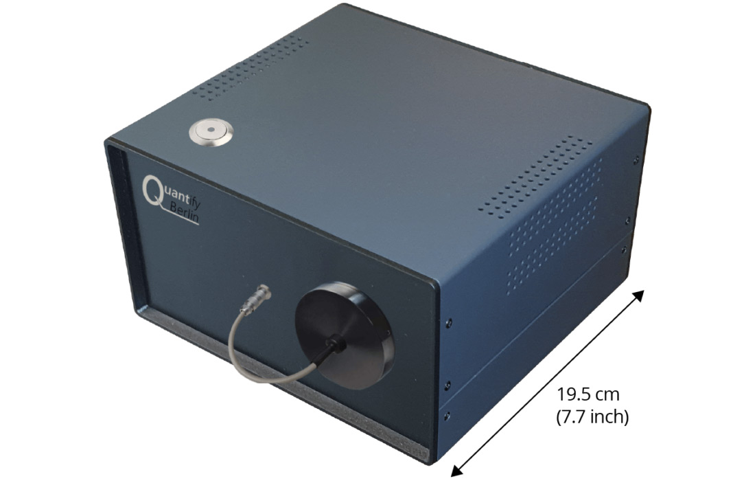
The "LumY Pro" measuring device is smaller than a shoe box (20x22x12 cm) and can also be used in the protective atmosphere of a glove box. It measures the quantity of photons or electrons being injected into a sample and the quantity of photons emitted by the excitation (absolute photon or electroluminescence). This enables researchers to draw conclusions about the charge carrier density in the absorber and to look in detail at where losses occur in the device or layer.

Measuring the quality of film absorbers, layer stacks and complete devices

Single layers, but also layer stacks and complete devices can be examined with flexibly adjustable light intensities and electrical voltages. The detailed analysis is integrated in a specially developed measuring and evaluation software. The software and the prototype of the system have already been successfully tested on various semiconductors in cooperation with the Helmholtz Innovation Lab HySPRINT.

Applicable for many semiconductor materials - evaluation software is included

LumY Pro can be used for the quality characterization of organic-inorganic perovskites, but also of other semiconductor materials such as kesterites or gallium arsenide. The development team hopes to accelerate the research and development of such opto-electronic devices and reduce the consumption of resources. The potential is great, because more than 400 research groups worldwide are working on solar cells made of perovskites alone.

"A precise measuring system that combines all these characterization possibilities is currently lacking on the market. We now want to implement this in a compact, versatile and yet easy to use product," says Dr. Lukas Kegelmann from the project team. The field study will now show how large the market potential is and which applications and functionalities are particularly interesting for users from research and industry.

LumY Pro was developed by scientists of the HZB groups around Dr. Thomas Unold, Dr. Eva Unger and Prof. Dr. Steve Albrecht.

  • Product flyer LumY Pro PDF (2.9 MB)


Contact

Dr. Lukas Kegelmann
Young Investigator Group Perowskite Tandem Solar Cells
Helmholtz-Zentrum für Materialien und Energie
Phone: +49 30 8062-41312
Email: lukas.kegelmann(at)helmholtz-berlin.de


Press release HZB, 19.06.2020

Analytics Research Microsystems / Materials Renewable Energies Photonics / Optics

Related News

LuQY Pro © QYB Quantum Yield Berlin

Faster development of efficient solar cells and LEDs thanks to LuQY Pro

HZB spin-off QYB Quantum Yield Berlin is launching a measurement instrument for optimising optoelectronic components
  • LinkedInshare0
  • Facebookshare0
  • WhatsAppshare0
  • E-Mail

The development of the Science and Technology Park Berlin Adlershof was and is co-financed by the European Union namely by EFRE. This concerns infrastructure development like construction of technology centres. Furthermore EFRE is used for international projects.

  • © WISTA Management GmbH
  • Legal Notice
  • Privacy Policy
  • Social Media Guide
  • FAQ
  • Contact
  • Press
  • Newsletter
  • RSS
  • International
Member of:
Zukunftsort Adlershof Logo