• Skip to Management
  • Skip to Main menu
  • Skip to Page content
Adlershof Logo
  • WISTA
  • WISTA.Plan
  • WISTA.Service
WISTA direkt
Search
  • de
  • en
  • Adlershof Logo
  • About / Directory
    • Companies / Institutes
    • Science City in numbers
    • Direction / Maps
      • Bus / Train
      • By Car
      • Bicycle
      • Orientation / Maps
      • Trail of Thoughts
  • Newsroom
    • Overview
    • News
      • Social Media Stream
      • Success Stories
    • Events / Calendar
      • Adlershof Dissertation Award
      • Adlershof Research Forum
      • Long Night of Sciences Berlin
    • Adlershof Journal
    • Hot Topics
      • Adlershof Mission "Grand Challenges"
      • Circular Economy
      • Digital infra­structure / 5G campus network
    • Photos / Flyer / Downloads
      • Magazine archive
    • WISTA-Editorial Staff
  • Science / Technology
    • Overview
    • Technology Centres
      • Photonics / Optics
      • Biotech­nology / Envi­ron­ment
      • Micro­systems / Materi­als
      • IT / Media
      • Renewable Energy / Photovoltaics
    • Non-university Research
    • Universities / Colleges
      • Humboldt-Universität zu Berlin
      • Services for Students
    • Young Talents / STEM / School Labs
    • Start-Ups
      • Adlershof Start-Up Centre IGZ
      • Adlershof Founder’s Lab
    • Networks / Management
      • Campus Club Adlershof
  • TV / Media
    • TV and Movie Production
    • Media Services / Companies
    • News and Events
    • Filming Locations
    • Costume Hire
    • GDR Film Archive
    • Tickets / Booking
  • Properties
    • Overview
    • Real Estate Rent
      • Office Space / Workspace / Laboratories
    • Real Estate Offers
      • Commercial Properties
    • ST3AM Working Environments / Coworking
    • Residential
    • Construction
      • Building Projects
      • Architecture
      • Webcam
  • Service
    • Overview
    • Gastronomy / Sport / Culture / Shopping
    • Jobs / Market
    • Social and Healthcare Facilities
    • WISTA-Business Services
    • Event Services / Guided Tours / Hotels
    • Facility Management
    • Downloads / Photos / Videos
    • Jobs for Refugees
  • Hood
    • Overview
    • History
    • Nature Park
    • Culture
    • Technology Park
    • Digital Tours
  • WISTA
  • WISTA.Plan
  • WISTA.Service
WISTA direkt

News

  • Overview
  • News
  • Events / Calendar
  • Adlershof Journal
  • Hot Topics
  • Photos / Flyer / Downloads
  • WISTA-Editorial Staff
  • Adlershof
  • Newsroom
  • News
17. September 2018

Patented nanostructure for solar cells

Rough optics, smooth surface

The nanostructure for capturing light is imprinted on silicon oxide (blue) and then "levelled" with titanium oxide (green). The result is an optically rough but smooth layer on which crystalline silicon can be grown. Picture: HZB

Thin-film solar cells made of crystalline silicon are inexpensive and achieve efficiencies of a good 14 percent. However, they could do even better if their shiny surfaces reflected less light. A team led by Prof. Christiane Becker from the Helmholtz-Zentrum Berlin (HZB) has now patented a sophisticated new solution to this problem

"It is not enough simply to bring more light into the cell," says Christiane Becker. Such surface structures can even ultimately reduce the efficiency by impairing the electronic properties of the material.

Rough and smooth
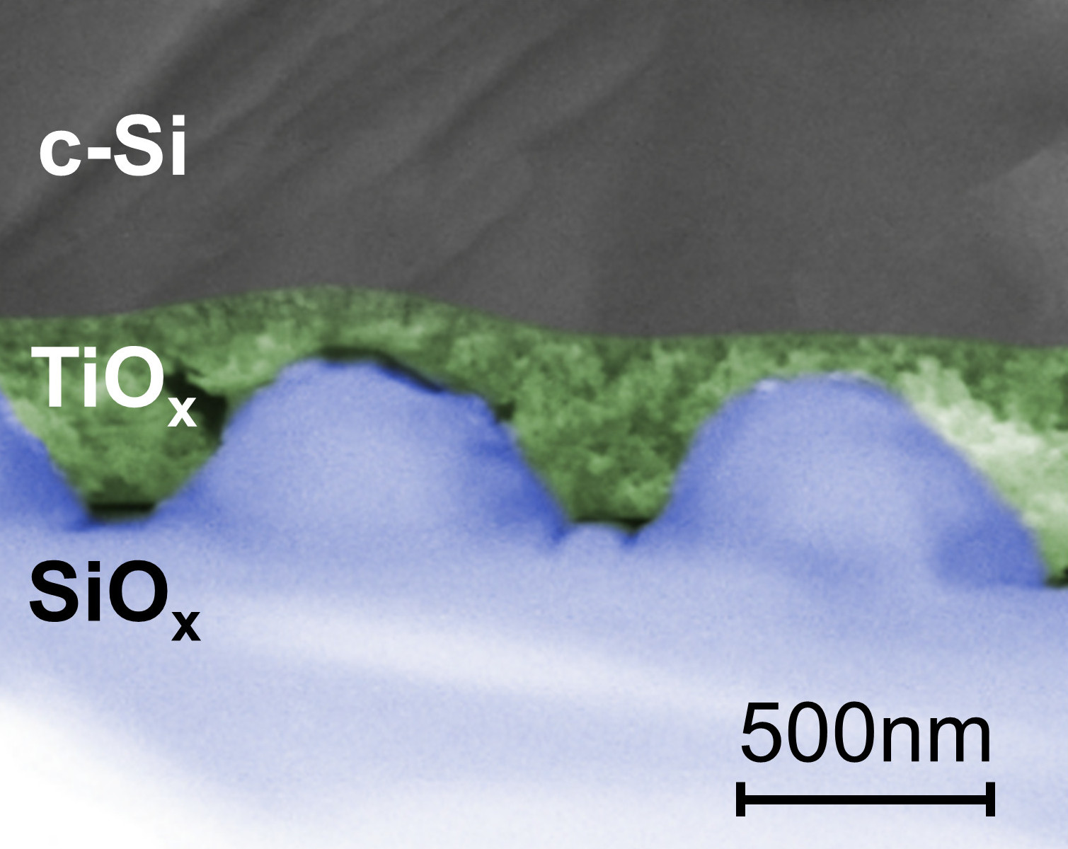
The idea that David Eisenhauer worked out as part of his doctorate in Becker's team sounds quite simple, but it requires a completely new approach: to produce a structure that behaves "optically rough" and scatters the light, but at the same time provides a "smooth" surface on which the silicon layer (the most important layer of the solar cell) can grow with virtually no defects.

Several steps for the SMART surface
The procedure consists of several steps: first, the researchers imprint an optimised nanostructure onto a still liquid silicon oxide precursor layer that is then cured with UV light and heat. This creates tiny, regularly arranged cylindrical elevations that are ideal for capturing light. However, the absorbing layer of crystalline silicon cannot grow flawlessly on this rough surface, so these structures have an unfavorable effect on the quality of the solar cell. In order to resolve this conflict, a very thin layer of titanium oxide is spin coated on top of the nanostructure in order to produce a relatively smooth surface on which the actual absorber material can be deposited and crystallized.

The coating has the descriptive name "SMART" for smooth anti-reflective three-dimensional texture. It reduces reflections and brings more light into the absorbing layer without impairing its electronic properties. The procedure is now patented.

Christiane Becker heads a Young Investigator Group at the HZB funded by the BMBF under the NanoMatFutur programme. As part of the BerOSE Joint Lab, she works closely with the Zuse Institute to use computer simulations for understanding the effects of nanostructuring on material properties.
 

Published in Scientific Reports (2017): Smooth anti-reflective three-dimensional textures for liquid phase crystallized silicon thin-film solar cells on glass; David Eisenhauer, Grit Köppel, Klaus Jäger, Duote Chen, Oleksandra Shargaieva, Paul Sonntag, Daniel Amkreutz, Bernd Rech & Christiane Becker


doi: 10.1038/s41598-017-02874-y


Contact:

Dr. Antonia Rötger
Tel: (030) 8062-43733
Fax: (030) 8062 - 42998
E-Mail: antonia.roetger(at)helmholtz-berlin.de

Renewable Energies Research Microsystems / Materials

Related News

  • photon upconversion © BAM/Christian Würth

    Efficient conversion of the wavelength

    By “upconversion” of photons, researchers at HZB and BAM achieve an up to a one-thousand-fold increase in the electric field strength of the light waves
  • CIGS Tandem scheme

    Thin-film tandem cells made of perovskite and CIGSe semiconductors

    Ultra-thin and extremely efficient solar cell due to new material combination
  • LinkedInshare0
  • Facebookshare0
  • WhatsAppshare0
  • E-Mail

The development of the Science and Technology Park Berlin Adlershof was and is co-financed by the European Union namely by EFRE. This concerns infrastructure development like construction of technology centres. Furthermore EFRE is used for international projects.

  • © WISTA Management GmbH
  • Legal Notice
  • Privacy Policy
  • Social Media Guide
  • FAQ
  • Contact
  • Press
  • Newsletter
  • RSS
  • International
Member of:
Zukunftsort Adlershof Logo