Perovskite solar cells: perfection not required!
Experiments at BESSY II reveal why even inhomogeneous perovskite films are highly functional
Metal-organic perovskite layers for solar cells are frequently fabricated using the spin coating technique. If you follow the simplest synthesis pathway and use industry-relevant compact substrates, the perovskite layers laid down by spin coating generally exhibit numerous holes, yet attain astonishingly high levels of efficiency. The reason that these holes do not lead to significant short circuits between the front and back contact and thus high-rate charge carrier recombination has now been discovered by a HZB team headed by Dr.-Ing. Marcus Bär in cooperation with the group headed by Prof. Henry Snaith (Oxford Univ.) at BESSY II.
The early metal-organic perovskites exhibited efficiency levels of only a few per cent (2.2 per cent in 2006). That changed quickly, however: the record level now lies considerably above 22 per cent. The equivalent efficiency increase in the current commercially dominant silicon solar cell technology took more than 50 years. The fact that thin films made of low cost metal-organic perovskites can be produced on a large scale for example by spin coating and subsequently baking (whereby the solvent evaporates and the material crystallizes), makes this technology additionally attractive.
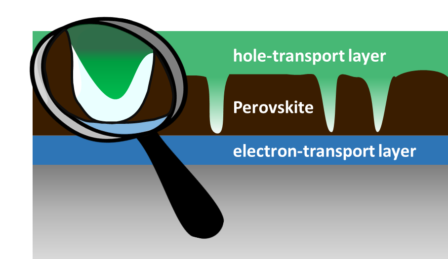
Holes in the perovskite film
Nevertheless, the thin perovskite film that results from spin coating on compact substrates is generally not perfect, but instead exhibits many holes. The samples from the pioneering perovskite group headed by Prof. Henry Snaith exhibit these holes as well. The problem is that these holes could lead to short circuits in the solar cell by the adjacent layers of the solar cell coming into contact. This would reduce the efficiency level considerably, which is not observed.
Thin layer is built up
Now Marcus Bär and his group, together with the Spectro-Microscopy group of the Fritz Haber Institute have carefully examined samples from Henry Snaith. Using scanning electron microscopy, they mapped the surface morphology. They subsequently analysed the sample areas exhibiting holes for their chemical composition using spectromicrographic methods at BESSY II. “We were able to show that the substrate was not really exposed even in the holes, but instead a thin layer is being built up essentially as a result of the deposition and crystallization processes there that apparently prevents short circuits”, explains doctoral student Claudia Hartmann.
.. and prevents short circuits
The scientists were able to ascertain at the same time that the energy barrier the charge carriers had to overcome in order to recombine with one another in the event of a direct encounter of the contact layers is relatively high. “The electron transport layer (TiO2) and the transport material for positive charge carriers (Spiro MeOTAD) do not actually come into direct contact. In addition, the recombination barrier between the contact layers is sufficiently high that the losses in these solar cells is minute despite the many holes in the perovskite thin-film”, says Bär.
The study is published in Advanced Materials Interfaces (2018): Spatially-resolved insight into the chemical and electronic structure of solution processed perovskites – why to (not) worry about pin-holes, C. Hartmann, G. Sadoughi, R. Félix, E. Handick, H. W. Klemm, G. Peschel, E. Madej, A. B. Fuhrich, X. Liao, S. Raoux, D. Abou-Ras, D. Wargulski, Th. Schmidt, R.G. Wilks, H. Snaith, and M. Bär
DOI: 10.1002/admi.201701420
Contact:
Helmholtz-Zentrum Berlin für Materialien und Energie
Prof. Dr. Marcus Bär
Young Investigator Group Interface Design
Tel.: (030) 8062-43824
Fax: (030) 8062-15641
Email: marcus.baer(at)helmholtz-berlin.de
Press Officer:
Dr. Antonia Rötger
Tel.: (030) 8062-43733
Fax: (030) 8062-42998
Email: antonia.roetger(at)helmholtz-berlin.de