Three-dimensional graphene
Experiment at BESSY II shows that optical properties are tuneable
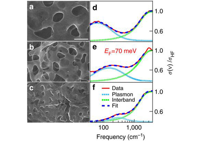
An international research team has for the first time investigated the optical properties of three-dimensional nanoporous graphene at the IRIS infrared beamline of the BESSY II electron storage ring. The experiments show that the plasmonic excitations (oscillations of the charge density) in this new material can be precisely controlled by the pore size and by introducing atomic impurities. This could facilitate the manufacture of highly sensitive chemical sensors.
Carbon is a very versatile element. It not only forms diamonds, graphite, and coal, but can also take a planar form as a hexagonal matrix – graphene. This material, consisting of only a single atomic layer, possesses many extreme properties. It is highly conductive, optically transparent, and is mechanically flexible as well as able to withstand loads. André Geim and Konstantin Novoselov received the 2010 Nobel Prize in Physics for the discovery of this exotic form of carbon. And just recently, a Japanese team has been successful in stacking two-dimensional graphene layers in a three-dimensional architecture with nanometre-sized pores.
Tuneable plasmons
A research team operated by a group at Sapienza University in Rome has now for the first time made a detailed investigation of the optical properties of 3D graphene at BESSY II. The team was able to ascertain from the data how charge density oscillations, known as plasmons, propagate in three-dimensional graphene. In doing so, they determined that these plasmons follow the same physical laws as 2D graphene. However, the frequency of the plasmons in 3D graphene can be very precisely controlled, either by introducing atomic impurities (doping), by the size of the nanopores, or by attaching specific molecules in certain ways to the graphene. In this way, the novel material might also lend itself to manufacturing specific chemical sensors, as the authors write in Nature Communications. In addition, the new material is interesting as an electrode material for employment in solar cells.
Advantages provided by the IRIS beamline
The researchers used the IRIS beamline at the BESSY II synchrotron source in Berlin to their advantage for their investigations. Broad-band infrared is available there, which especially facilitates spectroscopic analysis of novel materials using terahertz radiation. “A special operating mode of the BESSY II storage ring called low-alpha allowed us to measure the optical conductivity of three-dimensional graphene with a particularly high signal-to-noise ratio. This is hardly possible with standard methods, especially in the terahertz region. However, it is exactly this region that is important for observing critical physical properties”, says Dr. Ulrich Schade, head of the group at the infrared beamline.
Published in Nature Communications (2017): “Terahertz and mid-infrared plasmons in three-dimensional nanoporous graphene”; Fausto D’Apuzzo, Alba R. Piacenti, Flavio Giorgianni, Marta Autore, Mariangela Cestelli Guidi,Augusto Marcelli, Ulrich Schade, Yoshikazu Ito, Mingwei Chen & Stefano Lupi, DOI: 10.1038/ncomms1488
Contact
Helmholtz-Zentrum für Materialien und Energie
Dr. Ulrich Schade
Institute Methods for Material Development
Tel.: (030) 8062-13449
ulrich.schade(at)helmholtz-berlin.de
Press Officer
Dr. Antonia Rötger
Tel.: (030) 8062-43733
Fax: (030) 8062-42998
antonia.roetger(at)helmholtz-berlin.de