US patent for gallium oxide growth process of the IKZ
IKZ technology is protected in the world's most important markets
Power electronics based on beta-gallium oxide (ß-Ga₂O₃) is being intensively researched worldwide. The growth process developed at the IKZ yields large crystals with high quality and can be applied industrially. The technology is patented in Europe, South Korea and now, since June 2021, also in the U.S.
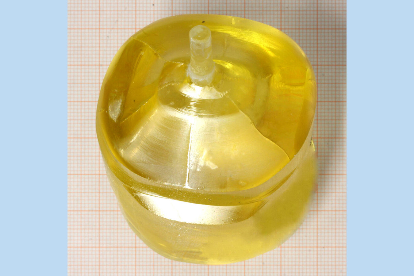
At the IKZ, not only research on crystal growth is carried out, but also new, commercially exploitable products are created. Substrates made of single-crystal semiconductor materials are the basis for electronic components such as computer chips, transistors and light-emitting diodes. ß-Ga2O3 is considered the future material for new and improved components in power electronics used in electric vehicles, wind turbines, current regulators, and other areas. Substrates are needed for this, but so far there are only a few manufacturers worldwide for ß-Ga2O3 crystals.
At the IKZ, Zbigniew Galazka has been researching the technology of a growth from the melt based on the Czochralski method for gallium oxide since 2009, in order to produce large volume crystals and from them substrates in various orientations [1-3]. These are now used worldwide to develop ß-Ga2O3 devices - including in the Leibniz Science Campus GraFOx, in which the IKZ plays a leading role. To secure the worldwide leading position in crystal growth technology, patents are an important asset. Following the patent application in January 2015, all negotiations have now been concluded and the IKZ technology is protected in the world's most important markets.
The crucial, patent-worthy step is to use a specific scheme of oxygen supply to keep the oxygen partial pressure in the growth system high enough to prevent the formation of elemental gallium in the melt and limit decomposition during the growth process, which is the key point for large-diameter crystals. At the same time, the oxygen partial pressure must be set low enough that the oxidation of expensive iridium crucible is minimized. The chosen process conditions / parameters and a smart furnace design create a suitable environment for the growth of ß-Ga2O3 single crystals from the melt. They ensure a stable crystal growth process and provide bulk ß-Ga2O3 crystals of high structural quality, suitable for homoepitaxy. The invention enables us to grow 2-inch diameter bulk β-Ga2O3 crystals with further scale-up capabilities. This technology can be applied to other growth methods and has already been transferred to other, thermally unstable oxides.
The patent "Method for growing beta phase of gallium oxide (ß-Ga2O3) single crystals from the melt contained within a metal crucible by controlling the O2 partial pressure" has been granted and published as Patent EP3242965B1 on June 26, 2019 in Europe and as Patent US11028501B2 on June 08, 2021 in the U.S. [4].
References:
[1] Z. Galazka, R. Uecker, K. Irmscher, M. Albrecht, D. Klimm, M. Pietsch, M. Brützam, R. Bertram, S. Ganschow, R. Fornari, „Czochralski growth and characterization of β-Ga2O3 single crystals“, Cryst. Res. Technol 45 (2010) 1229–1236
[https://doi.org/10.1002/crat.201000341]
[2] Z. Galazka, K. Irmscher, R. Uecker, R. Bertram, M. Pietsch, A. Kwasniewski, M. Naumann, T. Schulz, R. Schewski, D. Klimm, M. Bickermann, „On the Bulk β-Ga2O3 Single Crystals Grown by the Czochralski Method“, J. Crystal Growth 404 (2014) 184-191
[https://dx.doi.org/10.1016/j.jcrysgro.2014.07.021]
[3] Z. Galazka, R. Uecker, D. Klimm, K. Irmscher, M. Naumann, M. Pietsch, A. Kwasniewski, R. Bertram, S. Ganschow, M. Bickermann, „Scaling-up of Bulk β-Ga2O3 Single Crystals by the Czochralski Method“, ECS J. Solid State Sci. Technol. 6 (2017) Q3007-Q3011
[https://dx.doi.org/10.1149/2.0021702jss]
[4] Z. Galazka, S. Ganschow, D. Klimm, M. Bickermann, „Method for growing beta phase of gallium oxide (ß-Ga2O3) single crystals from the melt contained within a metal crucible by controlling the O2 partial pressure”, US Patent US11028501B2, published 08.06.21
[https://worldwide.espacenet.com/patent/search/family/052278525/publication/US11028501B2?q=US11028501B2]
Further information:
Leibniz-Institut für Kristallzüchtung im Forschungsverbund Berlin e.V.
Section Oxides & Fluorides
Zbigniew Galazka
Single Crystals of Oxide Semiconductors
Phone +49 30 6392 3020
Email zbigniew.galazka(at)ikz-berlin.de
Matthias Bickermann
Head of section
Phone +49 30 6392 3047
Email matthias.bickermann(at)ikz-berlin.de
Press release IKZ, 26 July 2021