The Plasma Start-up
Homogeneous layers and precise structuring for opto- and microelectronic components
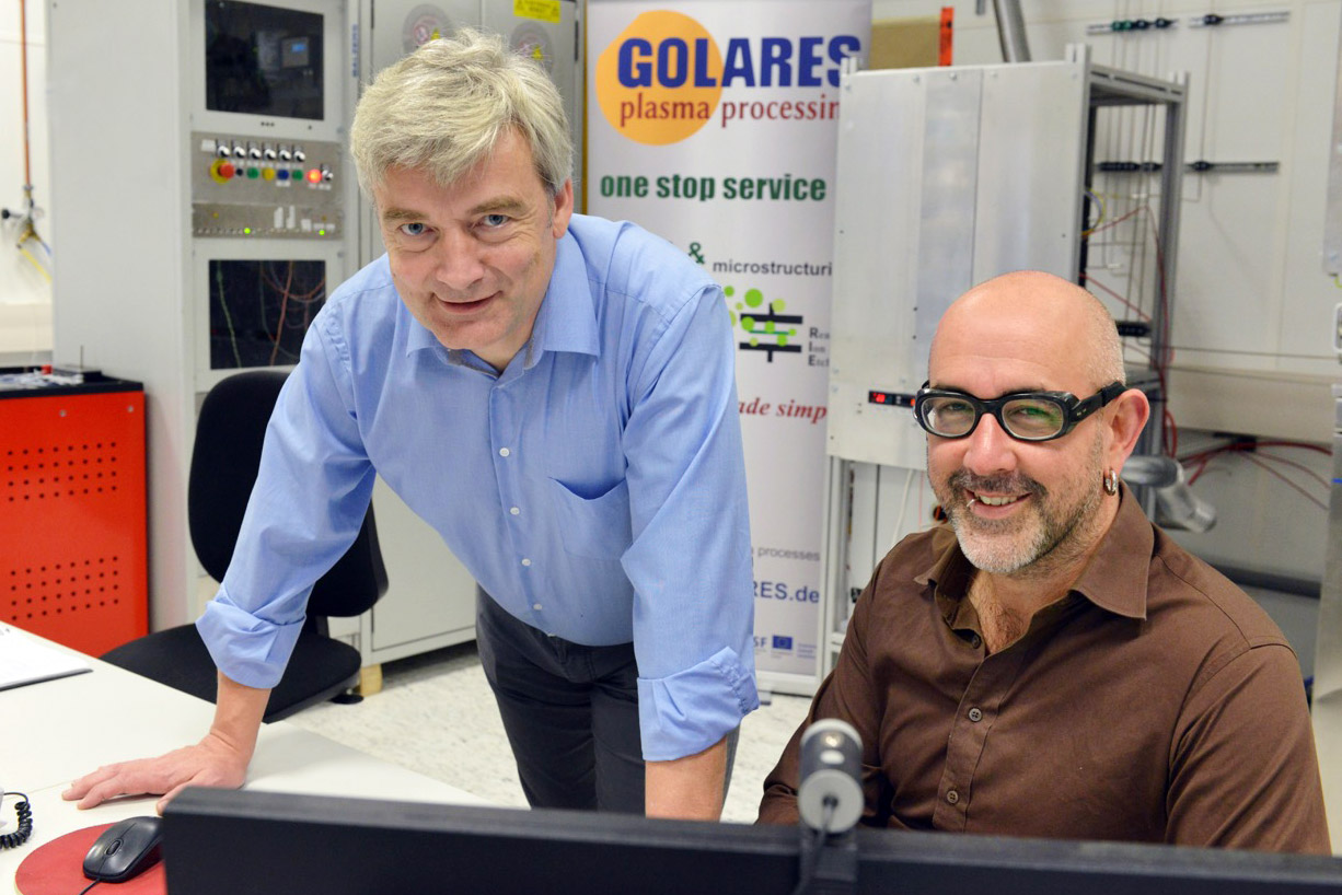
 Michael Arens and Sebastian Golka
The Golares GmbH is a newly established spin-off of the Leibniz-Institute for Crystal Growth (IKZ). At the Centre for Photonics and Optics in Adlershof, two founders are advancing a procedure for high-precision and homogeneous coating as well as efficient structuring of micro-optical components, sensors, and optoelectronic components using a self-developed plasma source.
When their stomachs start growling, Michael Arens and Sebastian Golka don’t always go out together. Arens loves beef roulades and light salads in summer. Golka prefers Asian cuisine. But as soon as the tables are cleared, the two founders of GOLARES GmbH put their heads together to refine their plasma procedure.
They have officially started being entrepreneurs in June 2016. Their business founding a few months before, which is secured by an EXIST start-up grant of the Federal Ministry for Economic Affairs and the European Social Fund. Their business plan is solid. They have succeeded in setting up their self-developed, inductively coupled plasma source in a disused facility. The two founders use it to structure or coat optoelectronic and microelectronic components. Sometimes it’s about heat dissipation of lasers, sometimes their plasma replaces wet chemical methods and burns structures into sensors or electro-optical components in a precise and dry process.
The possibilities this procedure creates are almost surreal. The plasma etches vertical trenches of a few nanometers into silicon wafers. Or it applies isolating and thermoconductive layers in order to mitigate heat problems in lasers and microsystems. This is possible because their facility produces plasma by means of an inductor through a glass sheet – in a vacuum at a pressure of one pascal. The advantage is that, under these conditions, the atoms are a thousand times further away from each other than under normal conditions. This pays off when the two founders funnel technical gases into the plasma depending on the application. Their molecules are chemically decomposed and ionised. “What matters is to distribute the energy to many atoms, instead of charging invidual atoms with high energy,” explains Golka. This is the only way to ensure that the functional layers cover the components in the reactor with great evenness, i.e. homogenously and with minimal surface roughness.
The type of layer is controlled by the two founders by means of the gas composition. They produce aluminium nitride from gas containing aluminium and nitrogen. Replace the aluminium with titanium and you get titanium nitride. Oxygen instead of nitride results in oxides. And so on. So far so good. But how does one etch trenches with vertical walls into components using plasma? – Arens is reluctant sharing the details, but concedes it has something to do with prestressing the components and lithographically applying protective masks to all those areas, which have to be protected from the etching gasses and remain unstructured. Additionally, the newly created walls of the nanometre trenches are coated with protective layers by using suitable gas mixtures. This way the plasma works its way down with a high selectivity and high etch rates to create highly defined trenches.
GOLARES can coat components up to eight inches and will soon also be able to structure them. These can be individual parts for research purposes or small batches. “Our procedure, its etch rates and the low levels of damage is considerably above the technological standard,” says Arens. Interested parties can approach the founders – and test the quality of the plasma processes free of charge. “We then support them to develop an optimised process for their requirements and application, create it in our facility and optimise it until the start of production,” he adds. It is certainly a great advantage that so many of their neighbours in Adlershof are active in microsystems technology. The only thing missing in the neighborhood is a similar supply of good Asian cuisine.
By Peter Trechow for Adlershof Journal