Printing an electronic rainbow
Combination of colour printing and chemical tunability enables printed spectrometer
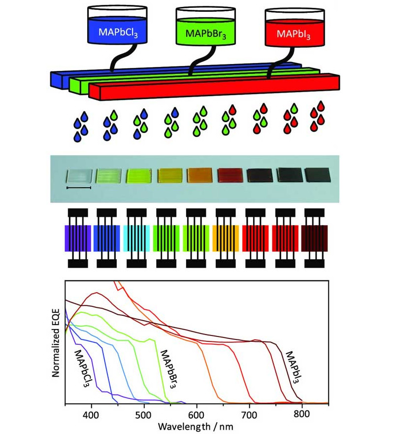
Researchers from Innovation Lab HySPRINT at Helmholtz-Zentrum Berlin (HZB) and IRIS Adlershof of Humboldt-Universität zu Berlin (HU) have used an advanced inkjet printing technique to produce a large range of photodetector devices based on a hybrid perovskite semiconductor. By mixing of only three inks, the researchers were able to precisely tune the semiconductor properties during the printing process. Inkjet printing is already an established fabrication method in industry, allowing fast and cheap solution processing. Extending the inkjet capabilities from large area coating towards combinatorial material synthesis opens the door for new possibilities for the fabrication of different kind of electronic components in a single printing step.
Wonder material metal halide perovskites
Metal halide perovskites are fascinating to researchers in academia and industry with the large range of possible applications. The fabrication of electronic components with this material is particularly appealing, because it is possible from solution, i.e. from an ink. Commercially available salts are dissolved in a solvent and then deposited on a substrate. The group around Prof. Emil List-Kratochvil, head of a joint research group at HZB and HU, focusses on building these types of devices using advanced fabrication methods such as inkjet printing. The printer spreads the ink on a substrate and, after drying, a thin semiconductor film forms. Combining multiple steps with different materials allows to produce solar cells, LEDs or photodetectors in mere minutes.
Inkjet printing is already an established technique in industry, not only for newspapers and magazines, but also for functional materials. Metal halide perovskites are specifically interesting for inkjet printing, as their properties can be tuned by their chemical make-up. Researcher at HZB have already used inkjet printing to fabricate solar cells and LEDs made from perovskites. The inkjet capabilities were further expanded in 2020, when the group of Dr. Eva Unger first used a combinatorial approach to inkjet printing, to print different perovskite compositions in search of a better solar cell material.
Combinatorial printing approach towards industrial production of electronic devices
Now, in this current work, the team around Prof. Emil List-Kratochvil found an exciting application for a large perovskite series within wavelength-selective photodetector devices. “Combinatorial inkjet printing cannot only be used to screen different compositions of materials for solar cell materials,” he explains, “but also enables us to fabricate multiple, separate devices in a single printing step.” Looking towards an industrial process, this would enable large scale production of multiple electronic devices. Combined with printed electronic circuits, the photodetectors would form a simple spectrometer: paper thin, printed on any surface, potentially flexible, without the need of a prism or grid to separate the incoming wavelengths.
Emil List-Kratochvil is Professor of Hybrid Devices at Humboldt-Universität zu Berlin, member of IRIS Adlershof and head of a Joint Lab founded in 2018 that is operated by HU together with HZB. In addition, a team jointly headed by List-Kratochvil and HZB scientist Dr. Eva Unger is working in the Helmholtz Innovation Lab HySPRINT at HZB on the development of coating and printing processes for hybrid perovskites. For a few days she is also an IRIS Adlershof-member.
Publication
Using Combinatorial Inkjet Printing for Synthesis and Deposition of Metal Halide Perovskites in Wavelength‐Selective Photodetectors
Vincent R. F. Schröder, Felix Hermerschmidt, Sabrina Helper, Carolin Rehermann, Giovanni Ligorio, Hampus Näsström, Eva L. Unger, Emil J. W. List-Kratochvil
Advanced Engineering Materials (2021), DOI: 10.1002/adem.202101111
Contact:
Prof. Dr. Emil List-Kratochvil
Helmholtz-Zentrum Berlin
Research Group Generative Manufacturing Processes for Hybrid Devices
Humboldt-Universität zu Berlin
Department of Physics | Department of Chemistry | IRIS Adlershof
AG Hybrid Devices
Phone +49 30 2093-7697
Email: emil.list-kratochvil(at)hu-berlin.de
Press release IRIS Adlershof, 22 December 2021