High-Performance Chips for Data Centres
Sicoya develops novel high-efficiency chips for transmitting data in data centres
The young Sicoya GmbH develops novel high-efficiency chips for transmitting data in data centres. Their silicon chips bring together optical and electrical circuitry. This will reduce costs, increase today’s 40 Gbit/s data transfer rates tenfold and significantly lower the energy use of data centres.
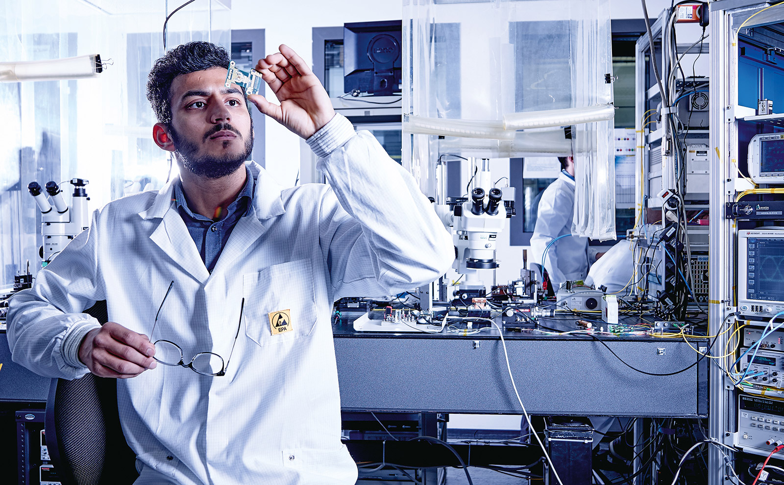
”Our product is the result of eight years of research and about 5.7 million euros in government funding,” says Torsten Fiegler, CFO of Sicoya GmbH. Two years after it was officially founded as a spin-off from Berlin’s Technical University, the company can look back on major achievements: its team has raised seven million euros in risk capital, while growing to 40 people. Unsurprisingly, there is a lot going on at the company headquarters at the Centre for Photonics and Optics in Adlershof. A multifarious mix of highly specialised employees, two thirds of which hold a PhD, works on computers or in clean room laboratories to advance novel chip designs. The company moved to Adlershof in January 2017. “A piece of good fortune!” as the company’s founders put it. Just before Christmas, the decision to move was final and the move-in took place three weeks later. It was facilitated by ample clean room space with antistatic flooring that the centre provides. It also provides ample room for expansion, which is consistent with the company’s rapid growth.
The company has already gained four customers. Two from Asia, one from Europe and one from the US. The start-up is aiming for a global billion-dollar market: data centres and data infrastructure. Online data traffic is growing exponentially due to streaming and cloud computing. For long distances, optical data transfer via glass fibre cables is the state of the art. For short distances inside data centres, however, copper cables are still widely used to save costs. This is where Sicoya’s innovative chips come into play.
“We combine optical and electrical circuits as well as modulators, which transform electrical into optical data signals, in one silicon chip,” says Sven Otte, the company’s CEO. The dimension where this takes place makes an ant seem like a giant: more than 10,000 of the above-mentioned modulators fit into one square millimetre. Overall, Sicoya’s chips and their photonic silicon circuitry measure four times three millimetres. This is crucial due to the limited space of the silicon wafers that the nano-scale structures are applied to. Shorter distances result in higher energy efficiency.
“Data centres account for about five percent of the overall energy use in the US,” says Otte. Even now that most large suppliers have moved their centres to cooler countries. The industry is seeking energy-efficient solutions to reduce energy costs and benefit the environment.
It is already quite clear that the start-up’s silicon photonics technology will be an immense success. Today’s copper-based technology achieves data transfer rates of 40 gigabits per second. Sicoya’s current generation of chips performs at 100 Gbit/s. As early as 2018, the design of the next generation will break the 400 Gbit/s barrier. Market researchers expect a big break. In just four years, the market segment, which the Adlershof-based founders are aiming for, will have grown to 2.5 billion dollars worldwide.
The team has recently concluded designing a new chip. The manufacturing process, which is done by the Frankfurt-based company IHP, consists of micro-structuring the wafers using a standardised procedure called BiCMOS, which takes up to a few months. “Before we deliver chips to our customers, we test them extensively in our clean room laboratories for a period of four to six weeks,” says the founder. The process chain consists of multiple steps, which also involves risk. Compared to current technology, however, Sicoya’s solution makes many suppliers and pre-production steps obsolete. “We are able to offer our chips using a disruptive price model,” says Fiegler. The founders are convinced that the total package they are offering will weigh out the risks of chip production. It is not every day that one is offered a tenfold performance improvement at significantly reduced costs and energy use.
By Peter Trechow for Adlershof Journal