HU research team develops new quantum sensor
Defects in the crystal lattice of materials can be measured in real time and with unprecedented precision
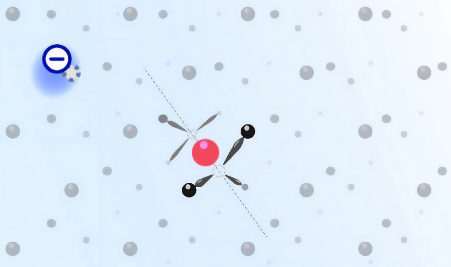
From computer chips to quantum dots—technological platforms such as these were only made possible thanks to a detailed understanding of the used solid-state materials, such as silicon or more complex semiconductor materials. This understanding also includes being able to identify and control irregularities in the crystal lattice of such materials. If, for example, an atom is missing in the lattice structure of the crystals, a single electron and thus an electric charge can become trapped there. Such charge traps generate electromagnetic noise that limits the functionality of these materials. However, it is extremely difficult to locate these charge traps on an atomic scale.
Researchers from the “Integrated Quantum Photonics” group at the Department of Physics at Humboldt-Universität zu Berlin (HU) and the “Joint Lab Diamond Nanophotonics” at the Ferdinand-Braun-Institut, led by Prof. Dr. Tim Schröder, have developed a new sensor that can detect such individual electrical charges more precisely than ever before. To achieve this, they relied on a defect in the crystal lattice — two vacancies combined with a foreign atom, which are also called color center because of their ability to absorb and emit light. It is already known that such optically-active color centers can be used as sensors to obtain information about material properties; however, the newly developed sensor allows individual electrical charges to be detected more precisely. To achieve this, such a color center was embedded in a rectangular material piece made out of artificial diamond.. The observation of the slightest changes in the color of the light emitted by the color center in the artificial diamond is the main mechanism for localizing the charge traps of individual electrons. The color center is characterized by a specific sensitivity to electric fields. If a single charge is captured near the sensor, the color changes are clearly visible; but if the charges are only a little further away, they cause almost no changes. This enables extremely precise determination of individual defects. In addition, the method allows real-time monitoring of the charges by repeating the measurement at regular intervals of up to one millionth of a second.
Patent application: Tool for materials science researchers in the quantum age
The researchers recently published a study demonstrating the properties of the sensor in the journal Nature Communications. They have also applied for a patent in Germany and the US for the method and device for locating charge traps in a crystal lattice. “This device is a new tool for researchers in materials science. It makes physical processes, which we were previously unable to observe, visible and helps us understand them. This is because we can now locate the interaction of charges with crystal defects much more precisely and can also record it much faster than before,” says Dr. Gregor Pieplow, who developed the software and methodological basis for the sensor. “The potential of the sensor goes way beyond that,” adds Cem Güney Torun, who worked on the design and setup of the experiment. “The integration of color centers into microscopic diamond tips will make it possible to analyze a wide variety of materials and realize a truly atomic, time-resolved, and fast scanning sensor.”
Further information:
- Link to the research article
- Link to the patent application in the USA
- Link to the patent application in Germany
Contact:
Humboldt-Universität zu Berlin
Department of Physics
Integrated Quantum Photonics Group
www.physics.hu-berlin.de/en/iqp
Dr. Gregor Pieplow
gregor.pieplow(at)physik.hu-berlin.de
Cem Güney Torun
toruncem(at)physik.hu-berlin.de
Prof. Dr. Tim Schröder
tim.schroeder(at)physik.hu-berlin.de
HU press release, 7 October 2025
