Novel Raman spectroscopy technique for investigation of thin films and surfaces
Enhanced surface-to-bulk Raman signal ratio using a transferable porous gold membrane
In a recent collaboration of the Emmy Noether Research Group "Physics of low-dimensional systems" around IRIS Adlershof member Dr. Sebastian Heeg at HU Berlin, researchers from the Leibniz-Institut für Kristallzüchtung (IKZ), the Université Le Mans, and the ETH Zurich, realized a novel modality in Raman spectroscopy through the development of surface-sensitive Raman scattering. This new approach addresses a major limitation of conventional Raman spectroscopy, where signals from surfaces or thin films are often weak and obscured by dominant bulk signals.
Surfaces play a pivotal role in science and industry as they are where most environmental interactions occur, including chemical reactions, adhesion, friction, and light interactions. Surface properties may differ significantly from bulk properties in terms of chemical composition, atomic arrangement, and electronic structure, influencing technological advancements such as catalysts and solar cells. Raman spectroscopy, a powerful, non-destructive technique for analysing molecular vibrations, provides insights into a material's chemical composition, crystallinity, defects, and strain. It is particularly valuable for characterising nanomaterials, thin films, and biological samples where precise surface information is essential.
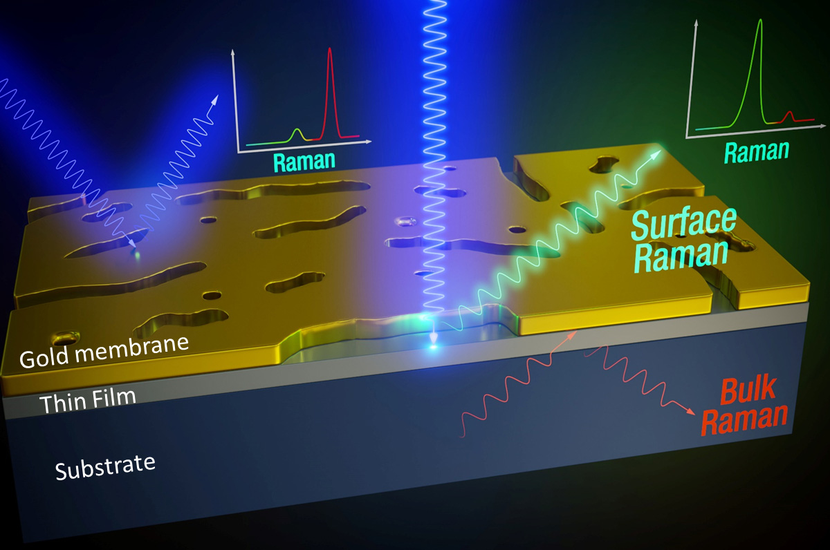
The application of conventional Raman spectroscopy to surfaces and thin films has been constrained by dominant bulk signals. However, using transferable porous gold membranes (PAuMs) allows for the study of surface-specific Raman signals with unprecedented clarity. PAuMs contain irregular, slot-shaped nanopores that act as plasmonic antennas. When placing PAuM on a surface or thin film of interest, the nanopores amplify the Raman signal of the surface directly below while the membrane itself suppresses bulk signals. Combining these effects improves the surface-to-bulk Raman signal ratio by three orders of magnitude and enables truly surface-sensitive Raman scattering.
The researchers used graphene as a model surface, observing that the nanopores in the membranes enhance the graphene Raman signal a hundredfold. Placing a spacer between graphene and the PAuM reveals that the Raman enhancement is confined to the first 2-3 nm of the material below the membrane, which demonstrates true surface sensitivity. A first prototypal application regards quantifying the strain in a 12.5 nm thin Si quantum well layer using PAuMs. The layer is part of a Silicon-Germanium heterostructure designed to use spin qubits as a promising and fast-developing technology for quantum computing.
In a second use-case, PAuMs are used to study the surface of thin LaNiO3 film, a metallic perovskite used as an electrode material. The electrical conductivity of LaNiO3 films is strongly coupled to its crystallographic structure and can be tuned by the film thickness. With PAuM placed on top of LaNiO3, the authors observed a Raman mode splitting arising from the film’s surface and indicating a difference in the surface structure compared to the bulk. This finding is consistent with theoretical predictions and observations from scanning tunnelling microscopy studies.
“Our work connects two separate fields” says Heeg, “Conceptually, we extend the field of plasmon-enhanced Raman spectroscopy, which is almost exclusively used to study and sense molecular compounds and nanostructures, to the field of solid states materials like Silicon quantum wells, thin complex oxides films, and related surfaces.” The team is now exploring the potential of the method with partners in Berlin and international collaborators. Dr. Pietro Marabotti, Einstein International Postdoctoral Fellow in Heeg’s group and co-author of the study, remarks that “our approach is not limited to crystalline surfaces, which we use as a showcase, but may also be used to study, for example, biological surfaces or surface-bound chemical reactions.” Researchers interested in the method are invited to get in touch with the team.
Publication:
Bulk-suppressed and surface-sensitive Raman scattering by transferable plasmonic membranes with irregular slot-shaped nanopores
Roman M. Wyss, Günther Kewes, Pietro Marabotti, Stefan M. Koepfli, Karl-Philipp Schlichting, Markus Parzefall, Eric Bonvin, Martin F. Sarott, Morgan Trassin, Maximilian Oezkent, Chen-Hsun Lu, Kevin-P. Gradwohl, Thomas Perrault, Lala Habibova, Giorgia Marcelli, Marcela Giraldo, Jan Vermant, Lukas Novotny, Martin Frimmer, Mads C. Weber, and Sebastian Heeg
Nat. Commun. 15, 5236 (2024). DOI: 10.1038/s41467-024-49130-2
Please read also the IKZ press release
Contact:
Dr. Sebastian Heeg
Humboldt-Universität zu Berlin
IRIS Adlershof & Department of Physics
+49 30 2093-82295
sebastian.heeg(at)physik.hu-berlin.de
www.physik.hu-berlin.de/en/pld
Source: IRIS Adlershof, 19 June 2024