Phosphorous chains – a 1D material with 1D electronic properties
One-dimensional electronic properties of a material were experimentally demonstrated for the first time at BESSY II
For the first time, a team at BESSY II has succeeded in demonstrating the one-dimensional electronic properties of a material through a highly refined experimental process. The samples consisted of short chains of phosphorus atoms that self-organise at specific angles on a silver substrate. Through sophisticated analysis, the team was able to disentangle the contributions of these differently aligned chains. This revealed that the electronic properties of each chain are indeed one-dimensional. Calculations predict an exciting phase transition to be expected as soon as these chains are more closely packed. While material consisting of individual chains with longer distances is semiconducting, a very dense chain structure would be metallic.
The material world consists of atoms that combine to manifold different substances. As a rule, atoms bond with each other both in one plane and perpendicular to it. However, some atoms such as carbon can also form graphene, a two dimensional (2D) hexagonal network in which they are connected only in one plane. Also, the element phosphorus can form stable 2D networks. 2D materials are an exciting area of research due to their amazing electronic and optical properties. Theoretical considerations suggest that the electro-optical properties of one-dimensional structures could be even more extraordinary.
Chains of Phosphorous atoms
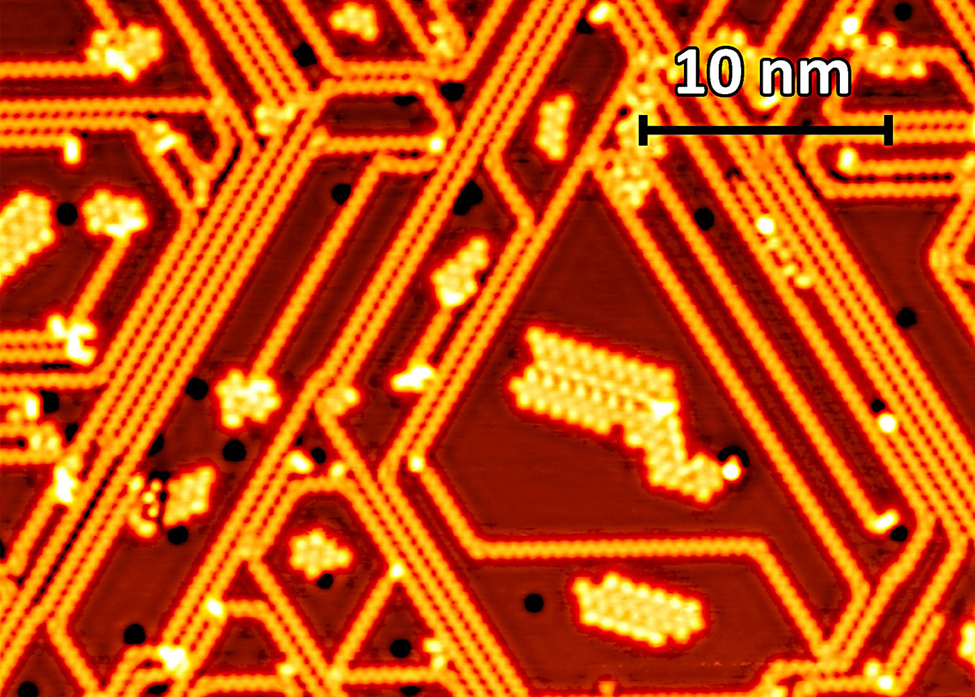
Recently it has become possible to produce one-dimensional structures: Under certain conditions phosphorus atoms do arrange themselves into short lines on a silver substrate. These chains are morphologically one-dimensional. However, it is likely that they interact laterally with other chains. Such interactions influence the electronic structure, potentially destroying the one-dimensionality. Until now, however, it has not been possible to measure this accurately in experiments.
‘Through a very thorough evaluation of measurements at BESSY II, we have now shown that such phosphorus chains really do have a one-dimensional electronic structure,’ says Professor Oliver Rader, head of the Spin and Topology in Quantum Materials department at HZB.
Dr Andrei Varykhalov and his team first produced and characterised phosphorus chains on a silver substrate using a cryogenic scanning tunnelling microscope (STM). The resulting images revealed the formation of short P chains in three different directions on the substrate, at 120 degree angles to each other.
ARPES at BESSY II shows 1D electronic structure
‘We achieved very high-quality results, enabling us to observe standing waves of electrons forming between the chains,’ says Varykhalov. The team investigated then the electronic structure using angle-resolved photoelectron spectroscopy (ARPES) at BESSY II, a method with which they already have a great deal of experience.
Phase transition with density predicted
Dr Maxim Krivenkov and Dr Maryam Sajedi did pioneering work here: By carefully analysing the data, they were able to distinguish the contributions of the three differently oriented phosphorus chains. ‘We could disentangle the ARPES signals from these domains and thus demonstrate that these 1D phosphorus chains actually possess a very distinct 1D electron structure too,’ says Krivenkov. Calculations based on density functional theory confirm this analysis and make an exciting claim: The closer these chains are to each other, the stronger their interaction. These results predict a phase transition from semiconductor to metal as the density of the chain array increases – as a conclusion, a two-dimensional phosphorus chain structure would be metallic.
‘We have entered a new field of research here, uncharted territory where many exciting discoveries are likely to be made,’ says Varykhalov.
Publication:
Small Structures (2025): Revealing the one-dimensional nature of electronic states in phosphorene chains
Maxim Krivenkov, Maryam Sajedi, Dmitry Marchenko, Evangelos Golias, Matthias Muntwiler, Oliver Rader and Andrei Varykhalov
DOI: 10.1002/sstr.202500458
Contact:
Helmholtz-Zentrum Berlin für Materialien und Energie
Department Spin and Topology in Quantum Materials
Dr. Maxim Krivenkov
(030) 8062-12345
maxim.krivenkov(at)helmholtz-berlin.de
apl. Prof. Dr. Oliver Rader
(030) 8062-12950
rader(at)helmholtz-berlin.de
Dr. Andrei Varykhalov
(030) 8062-14888
andrei.varykhalov(at)helmholtz-berlin.de
Press Officer:
Dr. Antonia Rötger
(030) 8062-43733
antonia.roetger(at)helmholtz-berlin.de
HZB press release, 21 October 2025