• Skip to Management
  • Skip to Main menu
  • Skip to Page content
Adlershof Logo
  • WISTA
  • WISTA.Plan
  • WISTA.Service
WISTA direkt
Search
  • de
  • en
  • Adlershof Logo
  • About / Directory
    • Companies / Institutes
    • Science City in numbers
    • Direction / Maps
      • Bus / Train
      • By Car
      • Bicycle
      • Orientation / Maps
      • Trail of Thoughts
  • Newsroom
    • Overview
    • News
      • Social Media Stream
      • Success Stories
    • Events / Calendar
      • Adlershof Dissertation Award
      • Adlershof Research Forum
      • Long Night of Sciences Berlin
    • Adlershof Journal
    • Hot Topics
      • Adlershof Mission "Grand Challenges"
      • Circular Economy
      • Digital infra­structure / 5G campus network
    • Photos / Flyer / Downloads
      • Magazine archive
    • WISTA-Editorial Staff
  • Science / Technology
    • Overview
    • Technology Centres
      • Photonics / Optics
      • Biotech­nology / Envi­ron­ment
      • Micro­systems / Materi­als
      • IT / Media
      • Renewable Energy / Photovoltaics
    • Non-university Research
    • Universities / Colleges
      • Humboldt-Universität zu Berlin
      • Services for Students
    • Young Talents / STEM / School Labs
    • Start-Ups
      • Adlershof Start-Up Centre IGZ
      • Adlershof Founder’s Lab
    • Networks / Management
      • Campus Club Adlershof
  • TV / Media
    • TV and Movie Production
    • Media Services / Companies
    • News and Events
    • Filming Locations
    • Costume Hire
    • GDR Film Archive
    • Tickets / Booking
  • Properties
    • Overview
    • Real Estate Rent
      • Office Space / Workspace / Laboratories
    • Real Estate Offers
      • Commercial Properties
    • ST3AM Working Environments / Coworking
    • Residential
    • Construction
      • Building Projects
      • Architecture
      • Webcam
  • Service
    • Overview
    • Gastronomy / Sport / Culture / Shopping
    • Jobs / Market
    • Social and Healthcare Facilities
    • WISTA-Business Services
    • Event Services / Guided Tours / Hotels
    • Facility Management
    • Downloads / Photos / Videos
    • Jobs for Refugees
  • Hood
    • Overview
    • History
    • Nature Park
    • Culture
    • Technology Park
    • Digital Tours
  • WISTA
  • WISTA.Plan
  • WISTA.Service
WISTA direkt

News

  • Overview
  • News
  • Events / Calendar
  • Adlershof Journal
  • Hot Topics
  • Photos / Flyer / Downloads
  • WISTA-Editorial Staff
  • Adlershof
  • Newsroom
  • News
12. September 2016

The best of both worlds

IRIS Scientists develop hybrid systems for optics and electronics

140 Scientists will work interdisciplinary at the new IRIS research facility with 4.500 square metres of lab and office space

What are the advanced materials supposed to have that the electronics of the future so desperately needs? “More speed, more brightness, more performance – and above all more multifunctionality,” replied Jürgen Rabe, Physics Professor at the Humboldt-Universität zu Berlin and chairman of IRIS (Integrative Research Institute for the Sciences) Adlershof. Silicon alone, the traditional material of semiconductor technology, can help to achieve these properties only with great difficulty. New substances must now be found that, for example, are electrically conducting, yet transparent, exhibit large areas, and yet are flexible. Set up in 2009 and now employing a workforce of about 100, the institute specialising in hybrid systems for optics and electronics took up this challenge.

”Our work involves combining the properties of classical semiconductors with those of advanced materials,” explained professor Rabe. Highly promising candidates are 2D materials like graphenes. Consisting of an ultra thin sheet of carbon atoms, this inorganic substance conducts electricity, is extremely resistant to tearing, and is also elastic. The material can be mixed over a large area with organic substances – molecules and polymers. Integrating nitrogen atoms lends the substance semiconductor properties. Recently, a group headed by Rabe was the first to manufacture this carbon nitride.

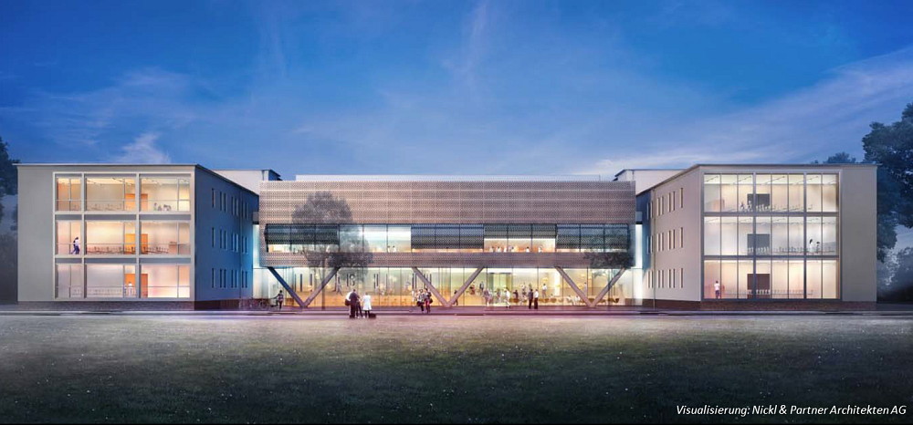
“We intend to utilise the short paths in Adlershof and also fetch new players on board,” claimed Rabe. Contributions will also be supplied by the new, adjoining research building whose completion is planned for 2018. Approximately 4500 square metres will provide the workspace for about 140 scientists dedicated to interdisciplinary research into organic-inorganic hybrid materials. These will include chemists, physicists, material scientists, and even theorists who are indispensable for the calculations involving macromolecules at the boundary surfaces.

Rabe also sees his team’s tasks in generating synergies between the understanding of scientific principles and their technical application in new products. This is helped by contacts with startups and established companies building up new lines of business and by joint ventures with strategic partners, also on the national and international levels. It therefore comes as no surprise that IRIS is one of the chief partners on the new material network INAM.

By Paul Janositz for Adlershof Special

www.iris-adlershof.de

  • LinkedInshare0
  • Facebookshare0
  • WhatsAppshare0
  • E-Mail

The development of the Science and Technology Park Berlin Adlershof was and is co-financed by the European Union namely by EFRE. This concerns infrastructure development like construction of technology centres. Furthermore EFRE is used for international projects.

  • © WISTA Management GmbH
  • Legal Notice
  • Privacy Policy
  • Social Media Guide
  • FAQ
  • Contact
  • Press
  • Newsletter
  • RSS
  • International
Member of:
Zukunftsort Adlershof Logo