• Skip to Management
  • Skip to Main menu
  • Skip to Page content
Adlershof Logo
  • WISTA
  • WISTA.Plan
  • WISTA.Service
WISTA direkt
Search
  • de
  • en
  • Adlershof Logo
  • About / Directory
    • Companies / Institutes
    • Science City in numbers
    • Direction / Maps
      • Bus / Train
      • By Car
      • Bicycle
      • Orientation / Maps
      • Trail of Thoughts
  • Newsroom
    • Overview
    • News
      • Social Media Stream
      • Success Stories
    • Events / Calendar
      • Adlershof Dissertation Award
      • Adlershof Research Forum
      • Long Night of Sciences Berlin
    • Adlershof Journal
    • Hot Topics
      • Adlershof Mission "Grand Challenges"
      • Circular Economy
      • Digital infra­structure / 5G campus network
    • Photos / Flyer / Downloads
      • Magazine archive
    • WISTA-Editorial Staff
  • Science / Technology
    • Overview
    • Technology Centres
      • Photonics / Optics
      • Biotech­nology / Envi­ron­ment
      • Micro­systems / Materi­als
      • IT / Media
      • Renewable Energy / Photovoltaics
    • Non-university Research
    • Universities / Colleges
      • Humboldt-Universität zu Berlin
      • Services for Students
    • Young Talents / STEM / School Labs
    • Start-Ups
      • Adlershof Start-Up Centre IGZ
      • Adlershof Founder’s Lab
    • Networks / Management
      • Campus Club Adlershof
  • TV / Media
    • TV and Movie Production
    • Media Services / Companies
    • News and Events
    • Filming Locations
    • Costume Hire
    • GDR Film Archive
    • Tickets / Booking
  • Properties
    • Overview
    • Real Estate Rent
      • Office Space / Workspace / Laboratories
    • Real Estate Offers
      • Commercial Properties
    • ST3AM Working Environments / Coworking
    • Residential
    • Construction
      • Building Projects
      • Architecture
      • Webcam
  • Service
    • Overview
    • Gastronomy / Sport / Culture / Shopping
    • Jobs / Market
    • Social and Healthcare Facilities
    • WISTA-Business Services
    • Event Services / Guided Tours / Hotels
    • Facility Management
    • Downloads / Photos / Videos
    • Jobs for Refugees
  • Hood
    • Overview
    • History
    • Nature Park
    • Culture
    • Technology Park
    • Digital Tours
  • WISTA
  • WISTA.Plan
  • WISTA.Service
WISTA direkt

News

  • Overview
  • News
  • Events / Calendar
  • Adlershof Journal
  • Hot Topics
  • Photos / Flyer / Downloads
  • WISTA-Editorial Staff
  • Adlershof
  • Newsroom
  • News
17. March 2020

3D nano-metrology with X-ray fluorescence and scattering techniques

PTB researchers develop new algorithm for the fast reconstruction of atom distributions in 3D nanostructured surfaces

Simulation of GIXRF maps © PTB
Simulation of GIXRF maps for inhomogeneous distribution offluorescent atoms within the lamellar grating structure. From (a) to (c): sketch of the structure; the green box depicts the localization of the dopant atoms. From (a‘) to (c‘): corresponding GIXRF maps. Credit © PTB

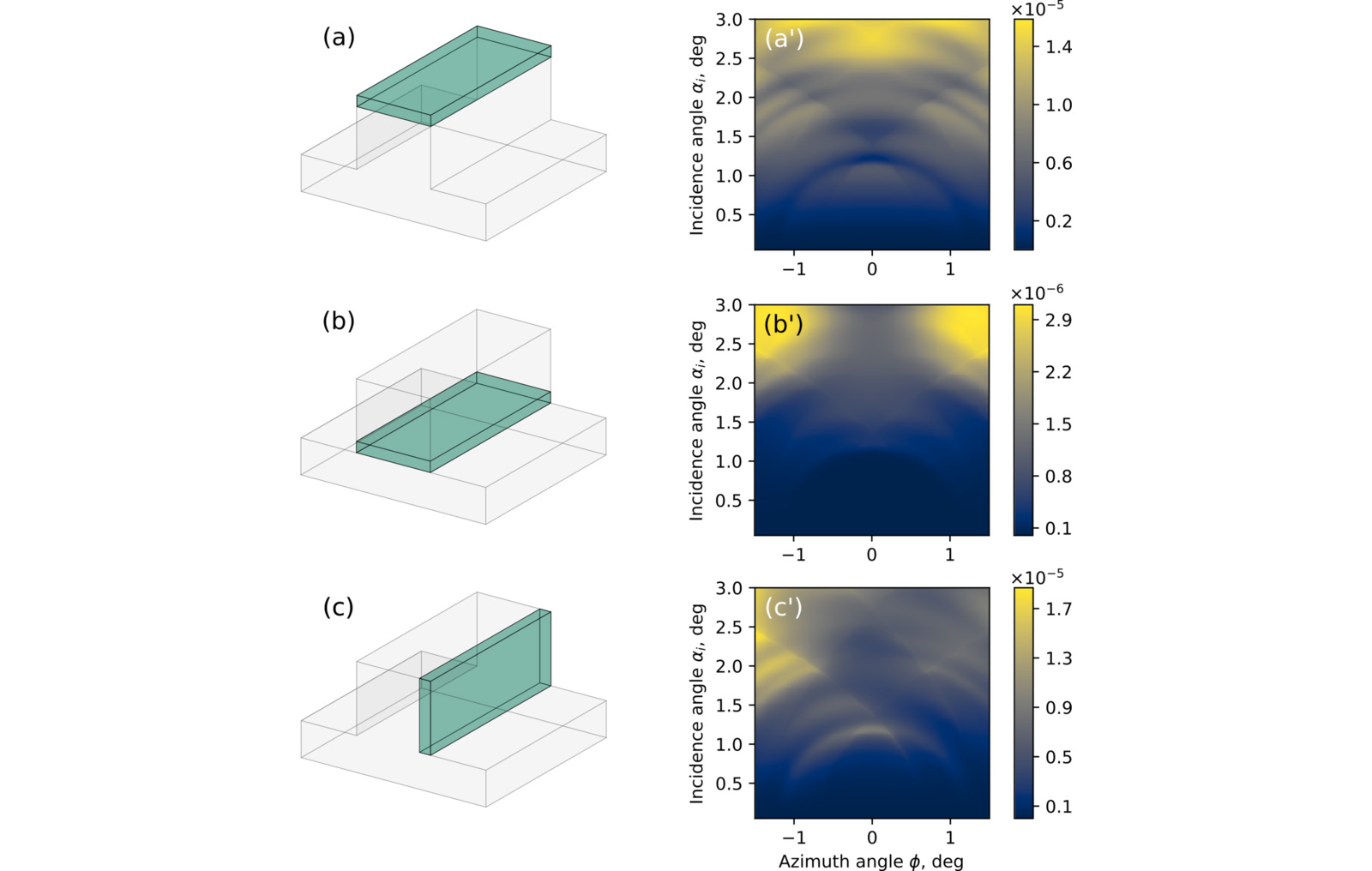
Over the last years, PTB has developed a new method for atom-specific reconstruction of periodically nanostructured surfaces. Recent studies have shown experimentally that it is possible to reconstruct and identify the spatial distribution of different atomic species in nano-components using X-ray fluorescence radiation. These techniques could become a powerful tool in the development and manufacture of nanostructures.

A new mathematical model for the simulation of X-ray fluorescence intensity at grazing incidence of periodic 3D nanopattern structures was developed in the working groups 7.14 (EUV-Nanometrology), 7.24 (X-ray Spectrometry) and 8.41 (Modelling and Simulation) in collaboration with the University of Twente and the Kurchatov Institute. The new algorithm can be applied in general for light-matter interactions of layered systems and nanostructures. It is more than one magnitude faster than conventional FEM solutions with similar precision and accuracy. The development of the simulation algorithm is a considerable step towards the application of high precision real-time measurements that are suitable for inline metrology needed for the control of flexible manufacturing processes. Moreover, the significant speed up of computations enables the determination of reliable uncertainties based on Bayesian approaches which opens the possibility for the development of hybrid metrology techniques to improve PTB’s measurement capabilities even further

Publication:

A semi-analytical approach for the characterization of ordered 3D nanostructures using grazing-incidence X-ray fluorescence, Nikolaev, K. V., Soltwisch, V., Hönicke, P., Scholze, F., de la Rie, J., Yakunin, S. N., Makhotkin, I. A., van de Kruijs, R. W. E. & Bijkerk, F. (2020). J. Synchrotron Rad. 27


Contact:

Physikalisch-Technische Bundesanstalt

Dr. Sebastian Heidenreich
Working group 8.41: Modelling and Simulation
Phone: +49 30 3481-7726
Email: sebastian.heidenreich(at)ptb.de

Victor Soltwisch
Working group 7.14: EUV-Nanometrology
Phone: +49 30 3481-7129
Email: victor.soltwisch(at)ptb.de

Philipp Hönicke
Working group 7.24: X-ray Spectrometry
Phone: +49 30 3481-7174
Email: philipp.hoenicke(at)ptb.de

www.ptb.de

Research Analytics Photonics / Optics

Related News

Fig. refractive index © PTB

Catalogue of optical constants of 19 materials in the EUV range published

PTB launches database to support the development of optical components in semiconductor industry

Related Institutions

  • Physikalisch-Technische Bundesanstalt PTB
  • LinkedInshare0
  • Facebookshare0
  • WhatsAppshare0
  • E-Mail

The development of the Science and Technology Park Berlin Adlershof was and is co-financed by the European Union namely by EFRE. This concerns infrastructure development like construction of technology centres. Furthermore EFRE is used for international projects.

  • © WISTA Management GmbH
  • Legal Notice
  • Privacy Policy
  • Social Media Guide
  • FAQ
  • Contact
  • Press
  • Newsletter
  • RSS
  • International
Member of:
Zukunftsort Adlershof Logo